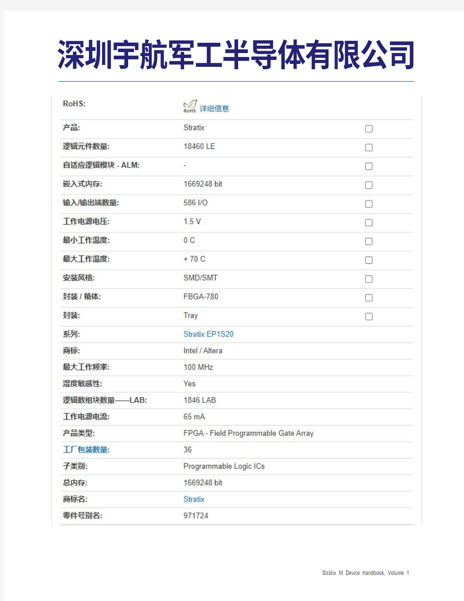
FPGA可编程逻辑器件芯片EP1S20F780C6N中文规格书
Chapter 11:Configuring Stratix III Devices
Passive Serial Configuration
If the Auto-restart configuration after error option is turned on, the devices release
their nSTATUS pins after a reset time-out period (maximum of 100μs). After all
nSTATUS pins are released and pulled high, the MAX II device can attempt to
reconfigure the chain without needing to pulse nCONFIG low. If this option is turned
off, the MAX II device must generate a low-to-high transition (with a low pulse of at
least 2μs) on nCONFIG to restart the configuration process.
1If you have enabled the Auto-restart configuration after error option, the nSTATUS pin transitions from high to low and back again to high when a configuration error is
detected. This appears as a low pulse at the nSTATUS pin with a minimum pulse width
of 10μs to a maximum pulse width of 500μs, as defined in the t STATUS specification.
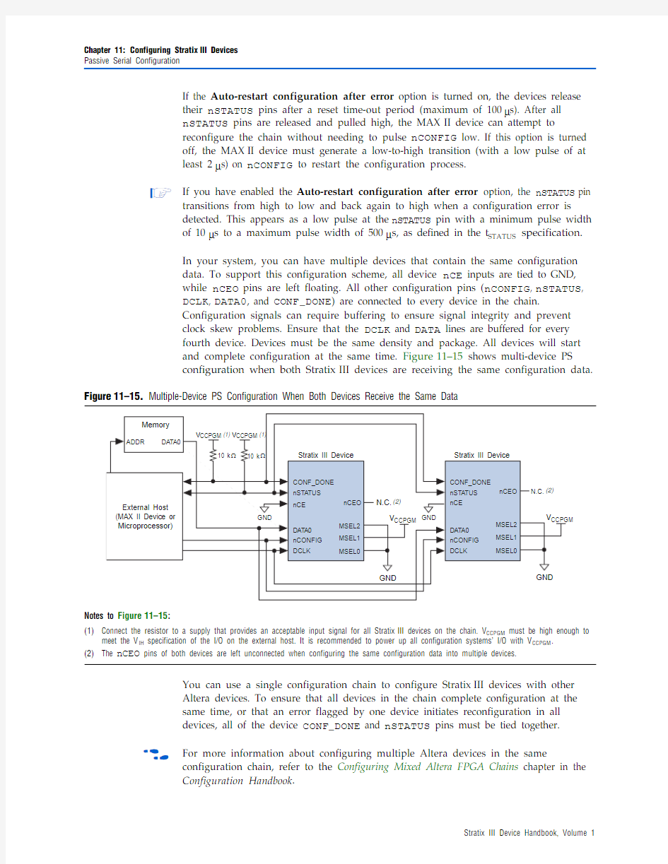
In your system, you can have multiple devices that contain the same configuration
data. To support this configuration scheme, all device nCE inputs are tied to GND,
while nCEO pins are left floating. All other configuration pins (nCONFIG, nSTATUS,
DCLK, DATA0, and CONF_DONE) are connected to every device in the chain.
Configuration signals can require buffering to ensure signal integrity and prevent
clock skew problems. Ensure that the DCLK and DATA lines are buffered for every
fourth device. Devices must be the same density and package. All devices will start
and complete configuration at the same time. Figure11–15 shows multi-device PS
configuration when both Stratix III devices are receiving the same configuration data. Figure11–15.Multiple-Device PS Configuration When Both Devices Receive the Same Data
Notes to Figure11–15:
(1)Connect the resistor to a supply that provides an acceptable input signal for all Stratix III devices on the chain. V CCPGM must be high enough to
meet the V IH specification of the I/O on the external host. It is recommended to power up all configuration systems’ I/O with V CCPGM.
(2)The nCEO pins of both devices are left unconnected when configuring the same configuration data into multiple devices.
You can use a single configuration chain to configure Stratix III devices with other
Altera devices. To ensure that all devices in the chain complete configuration at the
same time, or that an error flagged by one device initiates reconfiguration in all
devices, all of the device CONF_DONE and nSTATUS pins must be tied together.
f For more information about configurin
g multiple Altera devices in the same
configuration chain, refer to the Configuring Mixed Altera FPGA Chains chapter in the
Configuration Handbook.
Chapter 11:Configuring Stratix III Devices
Passive Serial Configuration
PS Configuration Timing
Figure 11–16 shows the timing waveform for PS configuration when using a MAX II device as an external host.
Table 11–10 defines the timing parameters for Stratix III devices for PS configuration.
Figure 11–16.PS Configuration Timing Waveform (Note 1)
Notes to Figure 11–16:
(1)The beginning of this waveform shows the device in user-mode. In user-mode, nCONFIG , nSTATUS , and CONF_DONE a re at logic high levels.
When nCONFIG is pulled low, a reconfiguration cycle begins.
(2)Upon power-up, the Stratix III device holds nSTATUS low for the time of the POR delay.(3)Upon power-up, before and during configuration, CONF_DONE is low .
(4)Do not leave DCLK floating after configuration. You should drive it high or low, whichever is more convenient. DATA[0] is available as a user
I/O pin after configuration. The state of this pin depends on the dual-purpose pin settings.
(5)Two DCLK falling edges are required after CONF_DONE goes high to begin the initialization of the device.
nCO N FIG
nSTATUS (2)
CO N F_DO N E (3)
DCLK DATA
User I/O
I N IT_DO N
E
t Table 11–10.PS Timing Parameters for Stratix III Devices (Part 1 of 2)
Chapter 11:Configuring Stratix III Devices Passive Serial Configuration
You can use a download cable to configure multiple Stratix III devices by connecting each device's nCEO pin to the subsequent device's nCE pin. The first device's nCE pin is connected to GND while its nCEO pin is connected to the nCE of the next device in the chain. The last device's nCE input comes from the previous device, while its nCEO pin is left floating. All other configuration pins (nCONFIG , nSTATUS , DCLK , DATA0, and CONF _DONE ) are connected to every device in the chain. Because all CONF _DONE pins are tied together, all devices in the chain initialize and enter user mode at the same time.
In addition, because the nSTATUS pins are tied together, the entire chain halts configuration if any device detects an error. The Auto-restart configuration after error option does not affect the configuration cycle because you must manually restart configuration in the Quartus II software when an error occurs.
Figure 11–17.PS Configuration Using a Download Cable
Notes to Figure 11–17:
(1)You should connect the pull-up resistor to the same supply voltage (V CCPGM ) as the USB-Blaster, MasterBlaster (V IO pin), ByteBlaster II,
ByteBlasterMV, or EthernetBlaster cable.
(2)You only need the pull-up resistors on DATA0 and DCLK if the download cable is the only configuration scheme used on your board. This ensures
that DATA0 and DCLK are not left floating after configuration. For example, if you are also using a configuration device, you do not need the pull-up resistors on DATA0 and DCLK .
(3)Pin 6 of the header is a V IO reference voltage for the MasterBlaster output driver. V IO should match the device's V CCPGM . Refer to the MasterBlaster
Serial/USB Communications Cable Data Sheet for this value. In the USB-Blaster, ByteBlaster II, ByteBlasterMV, or EthernetBlaster cable, this pin is a no connect.
G N D
V
Chapter 11:Configuring Stratix III Devices
Passive Serial Configuration
Figure 11–18 shows how to configure multiple Stratix III devices with a download cable.
f
For more information about how to use the USB-Blaster, MasterBlaster, ByteBlaster II, ByteBlasterMV , or EthernetBlaster cable, refer to the following user guides:
■USB-Blaster USB Port Download Cable User Guide ■MasterBlaster Serial/USB Communications Cable User Guide ■ByteBlaster II Parallel Port Download Cable User Guide ■
ByteBlasterMV Parallel Port Download Cable User Guide ■
EthernetBlaster Download Cable User Guide
Figure 11–18.Multi-Device PS Configuration using a Download Cable
Notes to Figure 11–18:
(1)Connect the pull-up resistor to the same supply voltage (V CCPGM ) as the USB-Blaster, MasterBlaster (V IO pin), ByteBlaster II, ByteBlasterMV, or
EthernetBlaster cable.
(2)You only need the pull-up resistors on DATA0 and DCLK if the download cable is the only configuration scheme used on your board. This is to
ensure that DATA0 and DCLK are not left floating after configuration. For example, if you are also using a configuration device, you do not need the pull-up resistors on DATA0 and DCLK .
(3)Pin 6 of the header is a V IO reference voltage for the MasterBlaster output driver. V IO should match the device's V CCPGM . Refer to the MasterBlaster
Serial/USB Communications Cable Data Sheet for this value. In the USB-Blaster, ByteBlaster II, ByteBlasterMV, or EthernetBlaster cable, this pin is a no connect.
10 k V
MEMORY存储芯片STM32F103C8T6中文规格书
Features ?ARM? 32-bit Cortex?-M3 CPU Core –72 MHz maximum frequency, 1.25 DMIPS/MHz (Dhrystone 2.1) performance at 0 wait state memory access –Single-cycle multiplication and hardware division ?Memories –64 or 128 Kbytes of Flash memory –20 Kbytes of SRAM ?Clock, reset and supply management – 2.0 to 3.6 V application supply and I/Os –POR, PDR, and programmable voltage detector (PVD) –4-to-16 MHz crystal oscillator –Internal 8 MHz factory-trimmed RC –Internal 40 kHz RC –PLL for CPU clock –32 kHz oscillator for RTC with calibration ?Low-power –Sleep, Stop and Standby modes –V BAT supply for RTC and backup registers ? 2 x 12-bit, 1 μs A/D converters (up to 16 channels) –Conversion range: 0 to 3.6 V –Dual-sample and hold capability –Temperature sensor ?DMA –7-channel DMA controller –Peripherals supported: timers, ADC, SPIs, I2Cs and USARTs ?Up to 80 fast I/O ports –26/37/51/80 I/Os, all mappable on 16 external interrupt vectors and almost all 5 V-tolerant ?Debug mode –Serial wire debug (SWD) & JTAG interfaces ?7 timers –Three 16-bit timers, each with up to 4 IC/OC/PWM or pulse counter and quadrature (incremental) encoder input –16-bit, motor control PWM timer with dead-time generation and emergency stop – 2 watchdog timers (Independent and Window) –SysTick timer 24-bit downcounter ?Up to 9 communication interfaces –Up to 2 x I2C interfaces (SMBus/PMBus) –Up to 3 USARTs (ISO 7816 interface, LIN, IrDA capability, modem control) –Up to 2 SPIs (18 Mbit/s) –CAN interface (2.0B Active) –USB 2.0 full-speed interface ?CRC calculation unit, 96-bit unique ID ?Packages are ECOPACK? Table 1. Device summary Reference Part number STM32F103x8 STM32F103C8, STM32F103R8 STM32F103V8, STM32F103T8 STM32F103xB STM32F103RB STM32F103VB, STM32F103CB, STM32F103TB 找Memory、FPGA、二三极管、连接器、模块、光耦、电容电阻、单片机、处理器、晶振、传感器、滤波器, 上深圳市美光存储技术有限公司 August 2015
20V转5V,20V转3.3V的LDO芯片规格书
40V高输入电压LDO线性稳压器一般说明 PW6206系列是一款高精度,高输入电压,低静态电流,高速,低压降线性稳压器具有高纹波抑制。在VOUT=5V&VIN=7V时,输入电压高达40V,负载电流高达300mA,采用BCD工艺制造。PW6206提供过电流限制、软启动和过热保护,以确保设备在良好的条件下工作 PW6206调节器有标准SOT89-3L和SOT23-3L封装。标准产品无铅无卤。 特点 ?输入电压:4.75V~40V ?输出电压:1.8V~5.7V ?输出精度:<±2% ?输出电流:150mA(典型值) ?最高300mA@VIN=7V,VOUT=5V,PW6206B50HV封装 ?电源抑制比:60dB@100Hz ?跌落电压:600mV@IOUT=100mA ?静态电流:4.2μA@VIN=12V(典型值) ?ESD HBM:8KV ?推荐电容器:10uF 应用芯片135代2845理8039 Mr。郑,技术工程FAE ?智能电表 ?车内娱乐 ?电动自行车 典型应用电路
应用信息 输入电容器 VIN 和GND 引脚之间需要10μF 的输入电容。电容器应尽可能靠近VIN 引脚,建议使用电解电容器。必须考虑公差和温度系数,以确保电容器在整个温度和工作条件范围内工作。 输出电容器
在实际应用中,选择输出电容器以保证其稳定运行是非常重要的。稳定和正确操作的最小电容为1μF。电容公差应在工作温度范围内±30%或更好。建议电容器类型为MLCC。 空载稳定性 PW6206将在无外部负载的情况下保持稳定和调节。这在CMOS RAM保持活动应用中尤其重要。 典型电路 下图显示了PW6206设备的典型应用电路。根据应用情况,应仔细选择外部组件的值。在插拔应用中,由于芯片上电源的插入和拔出引起的过冲会损坏芯片,因此建议VIN小于30V,输入电压峰值不超过45V。 在封堵应用中,建议R、Cin选用如下: 1Cin=10UF~100UF电解电容器,最大电压大于50V,R=0; 2Cin=1UF~10UF MLCC,最大电压V大于50V,R=2Ω,1206型电阻器应仔细选择,以确保有足够的裕度来承受插入期间的浪涌电流。
红外遥控器6122芯片规格书
WD6122 红外遥控发射电路 WD6122 芯片是通用红外遥控发射集成电路,采用CMOS 工艺制造,最多可外接64个按键,并有三组双重按键。封装形式为SOP-24和SOP-20。 一.特点 z低压CMOS 工艺制造 z工作电压范围宽 z通过外部接法最多可产生65536种用户码 z可通过SEL管脚选择,最多可支持128+ 6条指令码 z SOP-24、SOP-20、COB封装形式可选 二. 应用范围 z VCD、DVD 播放机、电视机、组合音响设备、电视机顶盒 三. 产品规格分类 z WD6122-001:SEL2接GND ,ROM中数据为0 z WD6122-002:SEL2接VDD,用户专用模式 四. 结构框图
WD6122 红外遥控发射电路 五. 管脚图及管脚说明 1. 管脚图 2. 管脚说明 管脚号 符号 输入输出 功能描述 23、24、1~6 KI0-KI7 I 键扫描输入端 7 REM O 数据输出管脚(遥控输出) 8 Vdd 电源正极 9 SEL I 选择管脚 10 OSCO O 振荡器管脚(输出) 11 OSCI I 振荡器管脚(输入) 12 Vss 电源负极 13 LMP O 输出LED指示(呈闪烁状态) 21~14 KI/O0~KI/O7I/O 键扫描输入/输出管脚 22 CCS I 键扫描输入
WD6122 红外遥控发射电路 六. 功能说明 1. 编码方式 WD6122 所发射的一帧码含有一个引导码,16位的用户编码和8位的键数据码、键数据码的反码也同时被传送。码型结构如下: 引导码由一个9ms的载波波形和4.5ms的关断时间构成,它作为随后发射的码的引导,这样当接收系统是由微处理器构成的时候,能更有效地处理码的接收与检测及其它各项控制之间的时序关系。编码采用脉冲位置调制方式(PPM)。利用脉冲之间的时间间隔来区分“0”和“1”。每次8位的码被传送之后,它们的反码也被传送,减少了系统的误码率。 2.键盘输入矩阵 WD6122键盘输入矩阵请参考下图: 3.按键输入 WD6122 在键扫描输入端KI0~KI7 和键扫描定时信号输入/输出端KI/O0~KI/O7构成的8×8 矩阵上共设置64 个按键。 只有第21#键与其它连在KI/O5 线上的键即22# 、23# 、24#键组合才能实现双重按键功能。即只有下列按键的组合才能进行双重按键操作。 1) 21#键与22#键;2 )21#键与23#键;3 )21#键与24#键 每个键输入端与电源负端VSS之间均接有下拉电阻。当有超过一个以上的按键(除非双重按键的组合21#与22#键21#与23#键21#与24#键)同时按下时,码的发射输出将停止。 当一个键按下时先读取用户码和键数据码,22ms后遥控输出端(REM)启动输出,按键时间只有超过22ms才能输出一帧码,超过108ms后才能输出第二帧码。 Edited by Foxit Reader Copyright(C) by Foxit Corporation,2005-2010For Evaluation Only.
普瑞45mil芯片规格书
Bridgelux BXCE 45x45 NLX-5 Product Data Sheet DS-C10 (2/4/2011) NLX-5 BLUE POWER DIE BXCE 45 x 45 mil PRODUCT DATA SHEET DS-C10 The Bridgelux NLX-5 family of blue power die enables high performance and cost effective solutions to serve solid state lighting market. This next generation chip technology delivers improved efficiency and performance to enable increased light output for a variety of lighting, signaling and display applications. Features ? High lumen output and efficiency ? Long operating life ? Increased current spreading traces for highly efficient and uniform illumination ? 100% Tested and sorted by wavelength, power and forward voltage ? Lambertian emission pattern ? Compatible with Solder paste, solder preform or silver epoxy die attach ? Delivered on medium tack blue tape (20cm±10mm ×20 cm±10mm) Applications ? General Illumination ? Street Lights ? Portable Lighting ? Architectural Lighting ? Directional Lighting ? Wide Area Lighting ? Display Backlighting ? Digital Camera Flash ? Automotive Lighting ? White LEDs LED Chip Diagram
TTP233D-HA6新版芯片规格书
单通道触摸感应开关 TTP233D-HA6 规格书 Revision 1.7 2014-04-25 一级代理:深圳市芯片科技有限公司芯派 深圳芯派科技 TEL:135 3045 2646 (唐生)ICQ:294 434 3362 ICQ:294 435 3362
1 key Touch Pad Detector IC Outline z The TTP233D-HA6 TonTouch TM is a touch pad detector IC which offers 1 touch key. The device built-in regulator for touch sensor. Stable sensing method can cover diversity conditions. The touching detection IC is designed for replacing traditional direct button key with diverse pad size. Low power consumption and wide operating voltage are the contact key features for DC or AC application. Characteristic z Operating voltage 2.4V ~ 5.5V z Built-in regulator for touch sensor z Built-in low voltage reset (LVR) function z Operating current, @VDD=3V no load At low power mode typical 2.5uA, maximum 5uA z The response time max about 220mS at low power mode @VDD=3V z Sensitivity can adjust by the capacitance(1~50pF)outside z Stable touching detection of human body for replacing traditional direct switch key z Provides Low Power mode z Provides direct output or toggle output selection by pin option (TOG pin) z Q pin is CMOS output can be selected active high or active low by pin option (AHLB pin) z Have the maximum on time 16 sec z After power-on have about 0.5sec stable-time, during the time do not touch the key pad, and the function is disabled z Auto calibration for life The re-calibration period is about 1 sec within 8 sec after power-on. When key has been touched within 8 sec or key has not been touched more than 8 sec after power-on, then the re-calibration period change to 4 sec Applications z Wide consumer products z Button key replacement
QJ003 芯片规格书
QJ003 芯片规格书 1.1 简介 QJ003 是一个提供串口的MP3芯片,完美的集成了MP3、WMV的硬解码。同时软件支持USB /SD/TF驱动,支持FAT16、FAT32文件系统。接播放USB/SD/TF 内部歌曲,直接从电脑USB下载进SD,使用方便,稳定可靠是此款产品的最大特点。另外该芯片也是深度定制的产品,专为USB读卡器,固定语音播放领域开发的低成本解决方案。 1.2 功能 1、支持采样率(KHz):8/11.025/12/16/22.05/24/32/44.1/48 2、24位DAC输出,动态范围支持90dB,信噪比支持85dB 3、完全支持FAT16、FAT32文件系统,最大支持32G的U盘、SD/TF 4、多种控制模式,红外遥控模式、AD按键控制模式 4、音频数据按文件夹排序,最多支持255个文件夹,每隔文件夹可以分配1000首歌曲 5、音量可调,5级EQ可调 6、连接电脑可以显示盘符进行更新内容; 7、在按键模式下,可以进行播放模式选择:单曲循环,大循环; 8、可连输入外部音源作声卡功能 9、LED随播放程闪烁状态 1.3 应用 1、车载导航语音播报 2、公路运输稽查、收费站语音提示; 3、火车站、汽车站安全检查语音提示; 4、电力、通信、金融营业厅语音提示; 5、车辆进、出通道验证语音提示; 6、公安边防检查通道语音提示; 7、多路语音告警或设备操作引导语音; 8、电动观光车安全行驶语音告示; 9、机电设备故障自动报警; 10、消防语音报警提示; 11、自动广播设备,定时播报
2 硬件参数 名称参数 MP3文件格式1、支持所有比特率11172-3和ISO13813-3 layer3音频解码 2、采样率支持(KHZ):8/11.025/12/16/22.05/24/32/44.1/48 3、支持Normal、Jazz、Classic、Pop、Rock等音效 USB接口 2.0标准 输入电压供电在3.3V-5.4V最佳为4.2V 额定电流15ma[不带U盘] 尺寸见6.芯片封装 工作温度-40度~70度 湿度5% ~ 95% 3.芯片管脚 管脚号管脚名称类型功能描述 1 P01 IO FLASH/TF数据脚 2 P00 IO FLASH/TF 时钟脚 3 P02 IO FLASH/TF 片选脚 4 VCOMO I ADKEY按键值检测脚 5 USBDM IO USB数据线DM 6 USBDP IO USB数据线DP 7 VCOM 芯片基准电压检测脚 8 DACVSS AGND 模拟地 9 DACR AO 芯片音源右声道输出 10 DACL AO 芯片音源左声道输出 11 VDDIO POWER 芯片LDO输出3.3V 12 LDO5V POWER 芯片电源输入引脚5V 13 VSSIO DGND 数字地 14 P23/24 AI 外部音源输入端 15 P30/P25 O LED工作状态指示灯,播放时间隔输出高低电平 16 P46/VPP I 遥控信号接收脚
芯片规格书
芯片规格书 芯片规格书是对每一个电子元器件的使用说明:关于芯片的封装规格,电流,电压,功能,包括IC原厂的信息。 ?在接触半导体行业以来,我记得有一个品牌(美国安霸)的规格书是要求需求方提供规格书的运用方案和查看规格书的资金的。可能很多同行的朋友对安霸这个品牌并不是很了解,安霸是全球做视频监控这块最大,技术最牛的一家半导体厂商。我们2013年的还帮一个北京的客户提供过安霸的芯片和规格书。因为我们有独特的渠道帮助客户解决了一个大问题。不过由于半导体近几年的发展,安霸厂商没有高的要求了。根据实际需求来说,规格书是每一个工程师都需要的,东西芯城的优势在于,我们的客服人员和销售人员可以帮助您解决寻找规格书的问题,还有就是东西芯城的特色功能参数搜索,可以很快的帮助同行和工厂的工程师解决选型和替代型号的问题。参数搜索:元器件类别,电流,电压,封装,还有运用范围。可以更快的帮助替换型号和选型的问题。工程是我们的企业DNA - 我们的工程背景意味着我们了解我们销售的产品,因此可以更好地与您合作,帮助您找到改善业务的机会。借助我们的工程实力,与IT团队的强强联手开发出了全球行业内的第一个智能元器件参数选型搜索引擎,以简化客户在选型过程中的甄选、对比工作。而且以我个人经验来说,我可以帮助很多同行的朋友来找找需求的芯片规格书。可以联系我们群号:136188203。半导体行业海外货源交流群,同时也为同行的或者工厂解决更多的半导体问题。 ?一个电子产品的定位:产品定位-工程画结构图-PCB画图-打样-选型-测试?电子产品的生产过程一般是这样的: 1、元器件进厂检验,PCB板进厂检验2、元器件成型处理,成型以便于插装。3、SMT贴片,经过回流焊接,将
JL1821S触摸芯片IC规格书(5键输出自锁)_V11
数据手册 DATASHEET JL1821S 5键(输出自锁)触摸感应芯片IC (Rev:1.1) 一、概述 JL1821S触摸感应IC是为实现人体触摸界面而设计的集成电路。可替代机械式轻触按键,实现防水防尘、密封隔离、坚固美观的操作界面。使用该芯片可以实现触摸开关控制,方案所需的外围电路简单,操作方便。确定好灵敏度选择电容, IC就可以自动克服由于环境温度、湿度、表面杂物等造成的各种干扰,避免由于电阻、电容误差造成的按键差异。
二、特点 1、高灵敏度(用户可自行调节) 2、高防水性能 3、待机功耗低,省电 4、高抗干扰性能,近距离、多角度手机干扰情况下,触摸响应灵敏度及可靠性不受影响 5、按键感应盘大小:大于3mm×3mm,根据不同面板材质跟厚度而定 6、按键感应盘间距:大于2mm 7、按键感应盘形状:任意形状(必须保证与面板的接触面积) 8、按键感应盘材料:PCB铜箔,金属片,平顶圆柱弹簧,导电橡胶,导电油墨,导电玻璃的ITO层等 9、面板材质:绝缘材料,如有机玻璃,普通玻璃,钢化玻璃,塑胶,木材,纸张,陶瓷,石材等 10、面板厚度:0~12mm,根据不同的面板材质有所不同 11、工作温度:-25℃~85℃ 12、工作电压:3V~5.5V 13、封装类型:SOP14 三、应用范围 1、消费类电子 2、数码产品 3、家用电器 4、小家电 四、封装及引脚定义 1、封装及引脚定义 JL1821S,SOP14 2、引脚定义描述 编号引脚定义功能描述编号引脚定义功能描述 1 VDD 电源正端8 KEY5 触摸按键输入脚5 2 KEY1 触摸按键输入脚1 9 OUT5 输出通道5
【免费下载】QJ003 芯片规格书
QJ003 芯片规格书1.1 简介 QJ003 是一个提供串口的MP3芯片,完美的集成了MP3、WMV 的硬解码。同时软件支持USB /SD/TF 驱动,支持FAT16、FAT32文件系统。接播放USB/SD/TF 内部歌曲,直接从电脑USB 下载进SD ,使用方便,稳定可靠是此款产品的最大特点。另外该芯片也是深度定制的产品,专为USB 读卡器,固定语音播放领域开发的低成本解决方案。1.2 功能1、支持采样率(KHz):8/11.025/12/16/22.05/24/32/44.1/482、24位DAC 输出,动态范围支持90dB ,信噪比支持85dB 3、完全支持FAT16、FAT32文件系统,最大支持32G 的U 盘、SD/TF 4、多种控制模式,红外遥控模式、AD 按键控制模式4、音频数据按文件夹排序,最多支持255个文件夹,每隔文件夹可以分配1000首歌曲5、音量可调,5级EQ 可调6、连接电脑可以显示盘符进行更新内容; 7、在按键模式下,可以进行播放模式选择:单曲循环,大循环;8、可连输入外部音源作声卡功能9、LED 随播放程闪烁状态1.3 应用1、 车载导航语音播报 2、 公路运输稽查、收费站语音提示; 3、 火车站、汽车站安全检查语音提示; 4、 电力、通信、金融营业厅语音提示; 5、 车辆进、出通道验证语音提示; 6、 公安边防检查通道语音提示; 7、 多路语音告警或设备操作引导语音; 8、 电动观光车安全行驶语音告示; 9、 机电设备故障自动报警; 10、消防语音报警提示; 11、自动广播设备,定时播报、管路敷设技术通过管线敷设技术,不仅可以解决吊顶层配置不规范问题,而且可保障各类管路习题到位。在管路敷设过程中,要加强看护关于管路高中资料试卷连接管口处理高中资料试卷弯扁度固定盒位置保护层防腐跨接地线弯曲半径标高等,要求技术交底。管线敷设技术中包含线槽、管架等多项方式,为解决高中语文电气课件中管壁薄、接口不严等问题,合理利用管线敷设技术。线缆敷设原则:在分线盒处,当不同电压回路交叉时,应采用金属隔板进行隔开处理;同一线槽内,强电回路须同时切断习题电源,线缆敷设完毕,要进行检查和检测处理。、电气课件中调试对全部高中资料试卷电气设备,在安装过程中以及安装结束后进行高中资料试卷调整试验;通电检查所有设备高中资料试卷相互作用与相互关系,根据生产工艺高中资料试卷要求,对电气设备进行空载与带负荷下高中资料试卷调控试验;对设备进行调整使其在正常工况下与过度工作下都可以正常工作;对于继电保护进行整核对定值,审核与校对图纸,编写复杂设备与装置高中资料试卷调试方案,编写重要设备高中资料试卷试验方案以及系统启动方案;对整套启动过程中高中资料试卷电气设备进行调试工作并且进行过关运行高中资料试卷技术指导。对于调试过程中高中资料试卷技术问题,作为调试人员,需要在事前掌握图纸资料、设备制造厂家出具高中资料试卷试验报告与相关技术资料,并且了解现场设备高中资料试卷布置情况与有关高中资料试卷电气系统接线等情况,然后根据规范与规程规定,制定设备调试高中资料试卷方案。、电气设备调试高中资料试卷技术电力保护装置调试技术,电力保护高中资料试卷配置技术是指机组在进行继电保护高中资料试卷总体配置时,需要在最大限度内来确保机组高中资料试卷安全,并且尽可能地缩小故障高中资料试卷破坏范围,或者对某些异常高中资料试卷工况进行自动处理,尤其要避免错误高中资料试卷保护装置动作,并且拒绝动作,来避免不必要高中资料试卷突然停机。因此,电力高中资料试卷保护装置调试技术,要求电力保护装置做到准确灵活。对于差动保护装置高中资料试卷调试技术是指发电机一变压器组在发生内部故障时,需要进行外部电源高中资料试卷切除从而采用高中资料试卷主要保护装置。
相关文档
- RH792A原版芯片规格书
- A2SHB单NMOS管芯片规格书
- IWATT 产品IW1692芯片规格书
- 2307三极管A7SHB芯片规格书PW2307
- 20V转5V,20V转3.3V的LDO芯片规格书
- 普瑞45mil芯片规格书
- SX6116芯片新版规格书
- PW2052 pdf降压芯片规格书
- ESP 芯片规格书
- 晶元芯片规格书
- QJ003 芯片规格书
- JL1821S触摸芯片IC规格书(5键输出自锁)_V11
- VC0703-Datasheet芯片规格书之数据手册
- LD1117芯片规格书
- A12芯片规格书
- FP7721芯片最新中文规格书
- LG芯片技术规格书_Rev0.1
- MEMORY存储芯片STM32F103C8T6中文规格书
- A2SHB三极管ic,A2SHB芯片 pdf规格书
- TTP233D-HA6新版芯片规格书