T4-4.3-P4

MICROCRYSTALLINE SILICON MATERIALS AND SOLAR CELLS WITH
HIGH DEPOSITION RATE
Xiaoyan Han, Xiaodan Zhang, Guofu Hou, Qunchao Guo, Yujie Yuan, Changchun Wei,
Jian Sun, Junming Xue, Ying Zhao, Xinhua Geng
Institute of photoelectronics thin film devices and technique of Nankai University.
Key Laboratory of photoelectronics thin film devices and technique of Tianjin.
Key Laboratory of Optoelectronic Information Science and Technology,
Ministry of Education. Tianjin, 300071, China
ABSTRACT
Although similar deposition rate (2.0nm/s) and defect absorption (α0.8eV =2.5cm-1) for intrinsic μc-Si:H films can be obtained at different total gas flow rate, the solar cell performance, which consists of the above intrinsic μc-Si:H as absorb layers, was obviously different. From the results of quantum efficiency (QE), dark J-V characteristic and Raman spectra, it was found that the amorphous silicon incubation layer is the main reason for the difference of the two solar cells. Increased the total gas flow rate can reduce the thickness of the amorphous silicon incubation layer, which can enhanced the QE response in the long wavelength and increase the short circuit current. These results demonstrate that the amorphous silicon incubation layer was a key factor for the fabrication of high efficiency microcrystalline silicon solar cell with high growth rate.
1. INTRODUCTION
Hydrogenated microcrystalline silicon (μc-Si:H), usually prepared by plasma-enhanced chemical vapor deposition (PECVD), draws much attention as a promising materials for thin film solar cells because of its spectral response at long wavelength and high stability against light exposure [1-3]. Yet, a μc-Si:H solar cell requires a rather thick intrinsic layer (﹥2.0μm) to sufficiently absorb the sunlight due to its indirect optical transition. Hence, high rate growth of μc-Si:H is a crucial issue for low-cost industrialization of solar cells[4-6]. However, high rate growth of the μc-Si:H is usually accompanied by a great number of dangling-bond (DB) defects in the resulting film, which act as recombination centers for photo-excited carriers, resulting in a deterioration in the device performance. So how to improve the quality of the films deposited at high rate becomes an important issue. However, some solar cells, which used the low defect density microcrystalline silicon materials as the intrinsic layers, not always obtain the better performance[7-8].
I n this study, we find that the intrinsic microcrystalline silicon thin films with a deposition rate as high as 2.0nm/s and defect absorption (α0.8eV is measured by CPM) as low as 2.5cm-1 can be obtained at different total gas flow rate. However, the J-V parameters of the solar cells which using the above intrinsic microcrystalline as their i-layers were obviously different. The reason for the above is discussed in this paper.
2. EXPERIMENT
The p, i, and n layers of the μc-Si:H solar cells were deposited in individual chambers of a cluster-tool deposition system by PECVD to form p-i-n single-junction diodes. The μc-Si:H p and i layers were deposited with VHF-PECVD at 60 and 70 MHz. The a-Si:H n layers were
Proceedings of ISES Solar World Congress 2007: Solar Energy and Human Settlement 1244
deposited with conventional RF-PECVD at 13.56 MHz.
The solar cell structure employed in this study was
glass/SnO2/ZnO-(textured)/p–i(1.5μm)–n/Al with an
active area of 0.253 cm2.
The solar cells have been tested by IV measurements in the
dark and under simulated solar light (AM1.5) using a
calibrated solar simulator. The solar cell parameters energy
conversion efficiency (η), short circuit current (Jsc), open
circuit voltage (Voc) and the fill factor (FF) of the diode
curve were deduced from the light IV curves, whereas the
diode quality factor (n) and the diode saturation current
density (J0) were deduced from the dark
I V curves.
Quantum efficiency spectra are used for information about the optical absorption and the charge-carrier extraction.
The optical absorption of the μc-Si:H intrinsic absorber layer of solar cells is measured by constant photocurrent method (CPM). For structural analysis, Raman spectroscopy was carried out on the intrinsic layer. Raman-scattering measurements with different excitation wavelengths (514nm (Ar+) and 633nm(He-Ne)) were introduced. The ratio of the integrated intensities of Gaussian peaks fitted to the Raman signal attributed to crystalline grains (at 500 and 520 cm-1) and disordered regions (480 cm-1), Xc= (I520+I500) / (I520+I500+I480) is used as a semi-quantitative value of the crystalline volume fraction.
3. RESULTS AND DISCUSSION
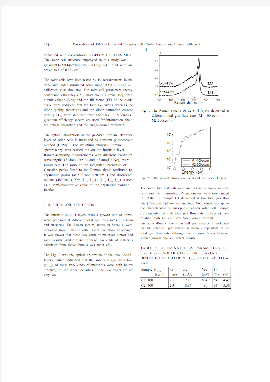
The intrinsic μc-Si:H layers with a growth rate of 2nm/s were prepared at different total gas flow rates (100sccm and 500sccm). The Raman spectra, shown in figure 1, were measured from film-side with 633nm excitation wavelength. It was shown that these two kinds of materials almost had same results. And the Xc of these two kinds of materials calculated from above formula was about 45%.
The Fig. 2 was the optical absorption of the two μc-Si:H layers, which indicated that the sub band gap absorption (α0.8eV) of these two kinds of materials were both below 2.5cm-1, i.e. the defect densities of the two layers are all very low.
350400450500550600
0.0
0.3
0.6
0.9
1.2
M2
Xc=44.5%
Xc=45%
I
n
t
e
n
s
i
t
y
(
a
.
u
.
)
Raman shift (cm-1)
M1
Fig. 1: The Raman spectra of μc-Si:H layers deposited at different total gas flow rate (M1-100sccm;
M2-500sccm).
10
10
10
10
10
Energy (ev)
α
(
c
m
-
1
)
Fig. 2: The optical absorption spectra of the μc-Si:H layer.
The above two materials were used as active layers in solar cells and the illuminated J-V parameters were summarized
in TABLE 1. Sample C1 deposited at low total gas flow
rate (100sccm) had low Jsc and high Voc, which was apt to
the characteristic of amorphous silicon solar cell. Sample
C2 deposited at high total gas flow rate (500sccm) have relative high Jsc and low Voc, which present microcrystalline silicon solar cell performance. It indicated
that the solar cell performance is strongly dependent on the
total gas flow rate although the intrinsic layers behave similar growth rate and defect density.
TABLE 1:
I
LLUM
I
NATED J-V PARAMETERS OF
μc-S
I
:H p-i-n SOLAR CELLS FOR i LAYERS DEPOSITED AT DIFFERENT F total (TOTAL GAS FLOW RATE)
Sample F total
(sccm)
Rd
(nm/s)
Jsc
(mA/cm2)
V oc
(mV)
FF
(%)
η
(%)
C1 100 2.1 12.16 684 54 4.47 C2 500 2.3 18.86 490 61 5.58
4 PV TECHNOLOGI ES, SYSTEMS AND APPLI CATI ONS
1245
A possibility to obtain information about transport and
recombination in the i layers and at the interfaces of the p -i -n μc-Si:H solar cells is the measurement of the dark J –V curves. In Fig. 3, the dark J –V curves of the solar cells of the C1 (100sccm) and C2 (500sccm) were shown exemplarily. With the decrease of F total a systematic shift of the curves to lower current densities can be observed. According to the simple p -n diode theory, if the validity of its application to μc-Si:H solar cells is assumed, the decrease in the current density qualitatively explains the increase of V OC . It means that the amorphous phase in C1 was more than C2 in spite of the two materials (M1, M2) had similar Xc.
D a r k c u r r e n t d e n s i t y (m A /c m 2
)
Voltage(V)
Fig. 3: The dark J –V curves of the solar cells in the C1
(100sccm) and C2 (500sccm). Besides the shift of the curves, a change of the slope in the exponential range is also observed. The diode factor n and saturation current density j 0 are calculated from the fitting of the exponential part of the dark J –V curves to the diode equation j dark = j 0[exp(eV/nkT)?1], where shunt and series resistances have minor influence on the dark current density. The results were plotted for the two solar cells in Fig. 3. With the decrease of the i -layer F total , the saturation current density j 0 increase. It indicated that the solar cell C1 had higher defect density than C2 when they had same intrinsic layer thickness. The diode factor n increase with decreasing F total , this shown that the bulk recombination in solar cell C1 is dominant.
I
n an attempt to study the influence of structure development on the carrier generation and transport, quantum efficiency measurements were performed on two
solar cells. In Fig. 4, the characteristic quantum efficiency (QE) spectrums of sample C1 and C2 were shown. Compared with C2, the QE spectrum of C1 exhibited low short wavelength response and almost no infrared response, implies the higher defect density in intrinsic layer, which act as recombination center of carriers. And maybe the amorphous silicon incubation layer was thicker in C1, which obstructed the carrier transport.
Q u a n t u m E f f i c i e n c y (a .u .)
Wavelength(nm)
Fig. 4: Quantum efficiency spectra of solar cells (samples
C1 and C2) prepared at different i-layer deposition F total .
In order to obtain more information about the structure of i-layers, Raman spectra are performed at different i-layer thickness on the same p-layer and shown in Fig. 5. The Raman excitation wavelength is 514nm, at which detection depth is about 150nm. t can be seen that when the thickness range from 200nm to 1500nm, the structure of films deposited with 100sccm flow rate starts from amorphous phase and then microcrystalline phase sets in with Xc of 60%. For the films deposited with 500sccm flow rate, all the films are microcrystalline phase. When the thickness range from 200nm to 1500nm, the Xc only increase from 33% to 63%. Therefore, the above results indicate that the amorphous silicon incubation layer of sample C1 is much thicker than that of C2. n fact, compared with the standard amorphous silicon, the amorphous silicon incubation layer had higher defect density, smaller band gap and lower absorption coefficient [9]. Thus, a thick incubation layer in solar cell will do harm to the carrier transport and deteriorate the cell performance in the end.
Proceedings of ISES Solar World Congress 2007: Solar Energy and Human Settlement
1246
R a m a n I n t e n s i t y (a .u .)
Raman shift(cm -1
)
0.00.2
0.4
0.6
0.8
1.0
R a m a n I n t e n s i t y (a .u .)
Raman shift(cm -1
)
Fig. 5: Raman spectrum detected at depth profile of the
intrinsic layers in two cells.
4. CONCLUSION
In this paper, the intrinsic microcrystalline silicon thin film with a deposition rate as high as 2.0nm/s and defect absorption (α0.8eV is measured by CPM) as low as 2.5cm -1 can be obtained at different total gas flow rate. However, the J-V parameters of the solar cells which using the above intrinsic microcrystalline as their i-layers were obviously different. From measurements of quantum efficiency (QE), dark J-V and micro-Raman scope, the results showed that the amorphous silicon incubation layer is the main reason for the difference of the two solar cells. Increased the total gas flow rate can reduce the thickness of the amorphous
silicon incubation layer, which can enhanced the QE response to the long wavelength and increase the short circuit current. As a result, solar cell with 5.58% efficiency has been achieved at deposition rate of 2.3 nm/s.
5. ACKNOWLEDGEMENTS
Project supported by National Natural Science Foundation of China (60506003), I
nternational cooperation project between China-Greece Government(2006DFA62390), the State Key Development Program for Basic Research of China (Grant No.2006CB202602, Grant No.2006CB 202603), Natural Science Foundation of Tianjin of China (05YFJMJC01600), the starting project of Nankai University (J02031), and the Program for New Century Excellent Talents in University of China (NCET).
6. REFERENCES
(1) Yang HD, Wu CY et al. Acta. Phys. Sin. 2003,52: 2865 (in Chinese)
(2) M. Kondo, T. Matsui, Y . Nasuno, et al. Thin Solid Films, 2006, 501 (1-2): 243 (3) Zhang XD, Zhao Y, et al. Acta. Phys. Sin. 2005,54(04) :1899 (in Chinese) (4) A. Shah, P. Torres, R. Tscharner, et al. Science, 1999, 285 (5428): 692
(5) S. Suzuki, M. Kondo, A. Matsuda, et al. Solar Energy Materials and Solar Cells, 2002, 74 (1-4): 489
(6) A. Madan and S. Morrison. Solar Energy Materials and Solar Cells, 1998, 55 (1-2): 127 (7) U.S.Graf, J.Meier, A.Shah. Photovoltaic Energy Conversion. 2003, 2: 1663
(8) Takuya Matsui, Akihisa Matsuda, Michio Kondo. Solar Energy Materials & Solar Cells. 2006,90: 3199
(9) A.J.M. Berntsen, W.F. van der Weg, P.A. Stolk, F.W. Saris, Phys.Rev. 1993, B 48:146