ADG3257BRQ-REEL7中文资料
High Speed, 3.3 V/5 V Quad 2:1 Mux/Demux
(4-Bit, 1 of 2) Bus Switch
ADG3257 Rev. E
Information furnished by Analog Devices is believed to be accurate and reliable. However, no re-
sponsibility is assumed by Analog Devices for its use, nor for any infringements of patents or other rights of third parties that may result from its use. Specifications subject to change without notice. No license is granted by implication or otherwise under any patent or patent rights of Analog Devices. T rademarks and registered trademarks are the property of their respective owners. One Technology Way, P.O. Box 9106, Norwood, M A 02062-9106, U.S.A. Tel: 781.329.4700 https://www.sodocs.net/doc/2f10703227.html, Fax: 781.461.3113 ?2002–2008 Analog Devices, Inc. All rights reserved.
2
9
1
4
-
1
FEATURES
100 ps propagation delay through the switch
2 Ω switches connect inputs to outputs
Data rates up to 933 Mbps
Single 3.3 V/5 V supply operation
Level translation operation
Ultralow quiescent supply current (1 nA typical) 3.5 ns switching
Switches remain in the off state when power is off Standard 3257 type pinout APPLICATIONS
Bus switching
Bus isolation
Level translation
Memory switching/interleaving FUNCTIONAL BLOCK DIAGRAM
1
2
1
2
1
2
1
2
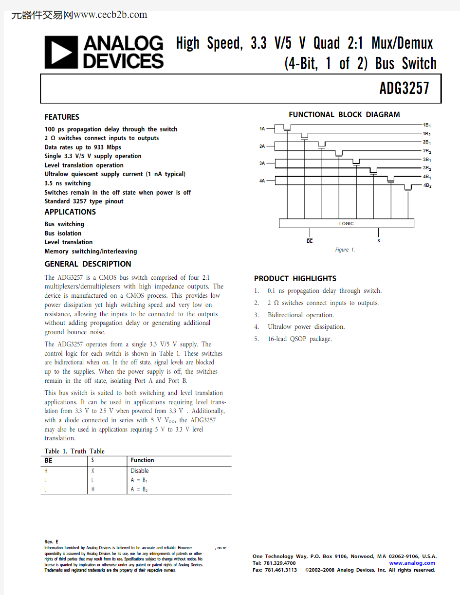
Figure 1.
GENERAL DESCRIPTION
The ADG3257 is a CMOS bus switch comprised of four 2:1 multiplexers/demultiplexers with high impedance outputs. The device is manufactured on a CMOS process. This provides low power dissipation yet high switching speed and very low on resistance, allowing the inputs to be connected to the outputs without adding propagation delay or generating additional ground bounce noise.
The ADG3257 operates from a single 3.3 V/5 V supply. The control logic for each switch is shown in Table 1. These switches are bidirectional when on. In the off state, signal levels are blocked up to the supplies. When the power supply is off, the switches remain in the off state, isolating Port A and Port B.
This bus switch is suited to both switching and level translation applications. It can be used in applications requiring level trans-lation from 3.3 V to 2.5 V when powered from 3.3 V. Additionally, with a diode connected in series with 5 V V DD, the ADG3257 may also be used in applications requiring 5 V to 3.3 V level translation.
PRODUCT HIGHLIGHTS
1.0.1 ns propagation delay through switch.
2. 2 Ω switches connect inputs to outputs.
3.Bidirectional operation.
4.Ultralow power dissipation.
5.16-lead QSOP package.
ADG3257
Rev. E | Page 2 of 12
TABLE OF CONTENTS
Features .............................................................................................. 1 Applications ....................................................................................... 1 Functional Block Diagram .............................................................. 1 General Description ......................................................................... 1 Product Highlights ........................................................................... 1 Revision History ............................................................................... 2 Specifications ..................................................................................... 3 Absolute Maximum Ratings ............................................................ 5 ESD Caution .................................................................................. 5 Pin Configuration and Function Descriptions ..............................6 Typical Performance Characteristics ..............................................7 Test Circuits ........................................................................................9 Applications Information .............................................................. 10 Mixed Voltage Operation, Level Translation .......................... 10 Memory Switching ..................................................................... 10 Outline Dimensions ....................................................................... 11 Ordering Guide .. (11)
REVISION HISTORY
03/08—Rev. D to Rev. E
Updated Format .................................................................... Universal Changes to Features .............................................................................1 Changes to General Description .......................................................1 Changes to Absolute Maximum Ratings ..........................................5 Changes to Pin Configuration and Function Descriptions ...........6 Changes to Test Circuits .....................................................................9 Changes to Ordering Guide ...............................................................11 11/04—Rev. C to Rev. D
Changes to Specifications ...................................................................2 Changes to Ordering Guide ...............................................................4 04/03—Rev. A to Rev. B
Updated Outline Dimensions ............................................................8 06/02—Rev. 0 to Rev. A
Edits to Features (1)
ADG3257
SPECIFICATIONS
V CC = 5.0 V ± 10%, GND = 0 V. All specifications T MIN to T MAX, unless otherwise noted.
1 Temperature range is: Version B: –40°C to +85°C.
2 See Test Circuits section.
3 All typical values are at T A = 25°C, unless otherwise noted.
4 Guaranteed by design, not subject to production test.
5 The digital switch contributes no propagation delay other than the RC delay of the typical R ON of the switch and the load capacitance when driven by an ideal voltage source. Because the time constant is much smaller than the rise/fall times of typical driving signals, it adds very little propagation delay to the system. Propagation delay of the digital switch, when used in a system, is determined by the driving circuit on the driving side of the switch and its interaction with the load on the driven side.
6 Propagation delay matching between channels is calculated from on-resistance matching of worst-case channel combinations and load capacitance.
7 This current applies to the control pins only and represents the current required to switch internal capacitance at the specified frequency. The A and B ports contribute no significant ac or dc currents as they transition.
Rev. E | Page 3 of 12
ADG3257
V CC = 3.3 V ± 10%, GND = 0 V. All specifications T MIN to T MAX, unless otherwise noted.
1 Temperature range is: Version B: ?40°C to +85°C.
2 See Test Circuits section.
3 All typical values are at T A = 25°C, unless otherwise noted.
4 Guaranteed by design, not subject to production test.
5 The digital switch contributes no propagation delay other than the RC delay of the typical R ON of the switch and the load capacitance when driven by an ideal voltage source. Because the time constant is much smaller than the rise/fall times of typical driving signals, it adds very little propagation delay to the system. Propagation delay of the digital switch, when used in a system, is determined by the driving circuit on the driving side of the switch and its interaction with the load on the driven side.
6 Propagation delay matching between channels is calculated from on-resistance matching of worst-case channel combinations and load capacitance.
7 This current applies to the control pins only and represents the current required to switch internal capacitance at the specified frequency. The A and B ports contribute no significant ac or dc currents as they transition.
Rev. E | Page 4 of 12
ADG3257
Rev. E | Page 5 of 12
ABSOLUTE MAXIMUM RATINGS
T A = 25°C, unless otherwise noted.
Table 4.
Parameter Rating
V CC to GND ?0.3 V to +6 V
Digital Inputs to GND ?0.3 V to +6 V
DC Input Voltage ?0.3 V to +6 V
DC Output Current
100 mA Operating Temperature Range
Industrial (B Version)
?40°C to +85°C Storage Temperature Range ?65°C to +150°C Junction Temperature 150°C QSOP Package
θJA Thermal Impedance 149.97°C/W Lead Soldering
Lead Temperature, Soldering (10 sec) 300°C IR Reflow, Peak Temperature (<20 sec) 220°C Soldering (Pb-Free)
Reflow, Peak Temperature 260(+0/?5)°C Time at Peak Temperature
20 sec to 40 sec
Stresses above those listed under Absolute Maximum Ratings may cause permanent damage to the device. This is a stress rating only; functional operation of the device at these or any
other conditions above those indicated in the operational sec-tion of this specification is not implied. Exposure to absolute
maximum rating conditions for extended periods may affect
device reliability.
ESD CAUTION
ADG3257
Rev. E | Page 6 of 12
PIN CONFIGURATION AND FUNCTION DESCRIPTIONS
1B 11B 21A
2B 22B 1S
BE 4B 14B 22A
3B 2ND 3A
3B 14A V CC 02914-002
G Figure 2. Pin Configuration
ADG3257
Rev. E | Page 7 of 12
TYPICAL PERFORMANCE CHARACTERISTICS
12
16
20
1
2
3
4
5
V A /V B (V)
R O N (?)
V A /V B (V)
Figure 3. On Resistance vs. Input Voltage
R O N (?)
00.5 1.0 1.5 2.0 3.0
2.5
Figure 4. On Resistance vs. Input Voltage
20
R O N (?)
1
2
3
4
5
V A /V B (V)
15
10
V A /V B (V)
R O N (?)
00.5 1.0 1.5 2.0 3.0
2.5Figure 5. On Resistance vs. Input Voltage for Different Temperatures 02914-006
Figure 6. On Resistance vs. Input Voltage for Different Temperatures
FREQUENCY (kHz)
C U R R E N T (A )
0.1
1101001k 10k
Figure 7. I CC
vs. Enable Frequency
INPUT VOLTAGE (V)
O U T P U T V O L T A G E (V )
012345
Figure 8. Maximum Pass Voltage
ADG3257
Rev. E | Page 8 of 12
O U T P U T V O L T A G E (V )
INPUT VOLTAGE (V)
00.5 1.0 1.5 2.0 2.5 3.0 3.5
Figure 9. Maximum Pass Voltage
Figure 10. 622 Mbps Eye Diagram
Figure 11. 933 Mbps Eye Diagram
ADG3257
Rev. E | Page 9 of 12
TEST CIRCUITS
V 2 × V CC 1PULSE GENERA TOR FOR ALL PULSES:t F <2.5ns,t R
<2.5ns.
2C L
= INCLUDES BOARD, STRA Y , AND LOAD CAP ACIT ANCES.3R T ISTHE TERMINA TION RESISTOR; SHOULD BE EQUAL TO Z OUT OF THE
PULSE GENERA TOR.
02914-012Figure 12. Load Circuit
IH
T
OH
T OL
02914-013
Figure 13. Propagation Delay
S1 @ 2V CC
S1 @ 2V CC
LOW
CONTROL INPUTS
OUTPUT OUTPUT 02914-014
Figure 14. Select, Enable, and Disable Times
Table 6. Switch S1 Condition
Test S1 t PLH , t PHL Open t PLZ , t PZL 2 × V CC t PHZ , t PZH GND t SEL
Open
Table 7. Test Conditions
Symbol
V CC = 5 V ± 10% V CC = 3.3 V ± 10% Unit R L 500 500 Ω ΔV 300 300 mV C L
50
50
pF
ADG3257
Rev. E | Page 10 of 12
APPLICATIONS INFORMATION
MIXED VOLTAGE OPERATION, LEVEL TRANSLATION
Bus switches can be used to provide a solution for mixed voltage systems where interfacing bidirectionally between 5 V and 3.3 V devices is required. To interface between 5 V and 3.3 V buses, an external diode is placed in series with the 5 V power supply as shown in Figure 15.
4-015
0291
Figure 15. Level Translation Between 5 V and 3.3 V Devices
The diode drops the internal gate voltage down to 4.3 V . The bus switch limits the voltage present on the output to
V CC ? External Diode Drop = V TH
Therefore, assuming a diode drop of 0.7 V and a V TH of 1 V , the output voltage is limited to 3.3 V with a logic high.
V
2.5V
2.5V
S W I T C H INPUT
IN
02914-016
Figure 16. Input Voltage to Output Voltage
Similarly, the device could be used to translate bidirectionally between 3.3 V to 2.5 V systems. In this case, there is no need for an external diode. The internal V TH drop is 1 V , so with a V CC = 3.3 V the bus switch limits the output voltage to
V CC ? 1 V = 2.3 V
V 3.3V 2.5V
2.5V
S W I T C H
INPUT
IN
02914-017
Figure 17. 3.3 V to 2.5 V Level Translation Using the ADG3257 Bus Switch
MEMORY SWITCHING
This quad bus switch may be used to allow switching between different memory banks, thus allowing additional memory and decreasing capacitive loading. Figure 18 illustrates the ADG3257 in such an application.
Figure 18. Allows Additional Memory Modules Without Added Drive or Delay
ADG3257
Rev. E | Page 11 of 12
COMPLIANT TO JEDEC STANDARDS MO-137-AB
OUTLINE DIMENSIONS
PLANE
0.0120.008
0.0100.006
0.0500.016
COPLANARITY
0.004
Figure 19. 16-Lead Shrink Small Outline Package [QSOP]
(RQ-16)
Dimensions shown in inches
ORDERING GUIDE
Model
Temperature Range Package Description
Package Option ADG3257BRQ
–40°C to +85°C 16-Lead Shrink Small Outline Package [QSOP] RQ-16 ADG3257BRQ-REEL –40°C to +85°C 16-Lead Shrink Small Outline Package [QSOP] RQ-16 ADG3257BRQ-REEL7 –40°C to +85°C 16-Lead Shrink Small Outline Package [QSOP] RQ-16 ADG3257BRQZ 1
–40°C to +85°C 16-Lead Shrink Small Outline Package [QSOP] RQ-16 ADG3257BRQZ-REEL 1 –40°C to +85°C 16-Lead Shrink Small Outline Package [QSOP] RQ-16 ADG3257BRQZ-REEL71
–40°C to +85°C 16-Lead Shrink Small Outline Package [QSOP] RQ-16
1
Z = RoHS Compliant Part.
ADG3257
Rev. E | Page 12 of 12
NOTES
?2002–2008 Analog Devices, Inc. All rights reserved. Trademarks and registered trademarks are the property of their respective owners. D02914-0-3/08(E)