RD151TS3312ARPH0中文资料

RD151TS3312ARP, RD151TS3322ARP Spread Spectrum Clock for EMI Solution
REJ03D0793-0100
Rev.1.00
May 11, 2006 Description
RD151TS3312ARP and RD151TS3322ARP is a high-performance Spread Spectrum Clock generator. It is suitable for EMI solution of electric systems.
Features
? Supports 10 MHz to 20 MHz operations. Multiple rate (XIN: SSCOUT) = 1: 1
Input frequency 10 MHz to 20 MHz
? Spread spectrum modulation ; RD151TS3312ARP : ±1.5%, ±0.5% (Central spread modulation)
RD151TS3322ARP : –3.0%, –1.0% (Down spread modulation)
Key Specifications
? Supply voltages: V DD = 3.3 V ±0.3 V
? Cycle to cycle jitter = ±100 ps typ.
? Clock output duty cycle = 50 ±5%
? Output slew rate = 0.7 V/ns typ.
? Ordering Information
Part Name Package Type
Package Code
(Previous Code)
Package
Abbreviation
Taping Abbreviation
(Quantity)
RD151TS3312ARPH0 RD151TS3322ARPH0 SOP-8 pin
(JEDEC)
PRSP0008DD-C
(FP-8DCV)
RP H (2,500 pcs / Reel)
Block Diagram
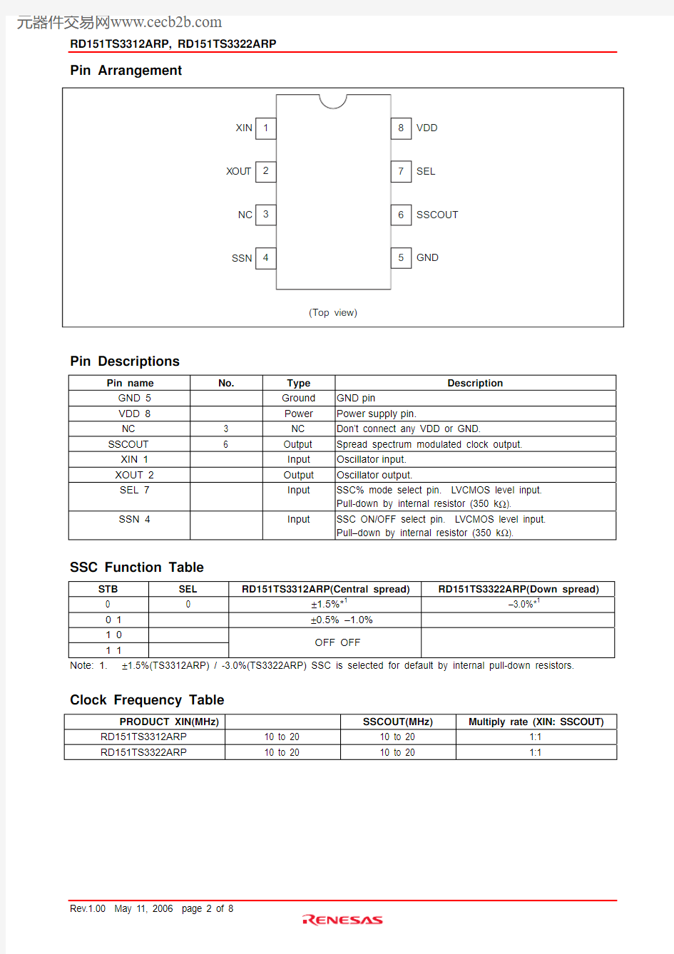
Pin Arrangement
Pin Descriptions
Pin name No. Type Description
pin
GND
GND 5
Ground
pin.
supply
Power
VDD 8
Power
NC 3 NC Don’t connect any VDD or GND.
SSCOUT 6 Output Spread spectrum modulated clock output.
input.
Oscillator
XIN 1
Input
Oscillator
output.
Output
XOUT 2
Input
SEL 7
SSC% mode select pin. LVCMOS level input.
Pull-down by internal resistor (350 k?).
Input
SSN 4
SSC ON/OFF select pin. LVCMOS level input.
Pull–down by internal resistor (350 k?).
SSC Function Table
STB SEL RD151TS3312ARP(Central spread) RD151TS3322ARP(Down spread)
0 0 ±1.5%*1 –3.0%*1
0 1 ±0.5% –1.0%
1 0
OFF OFF
1 1
Note: 1. ±1.5%(TS3312ARP) / -3.0%(TS3322ARP) SSC is selected for default by internal pull-down resistors.
Clock Frequency Table
Multiply rate (XIN: SSCOUT)
SSCOUT(MHz)
PRODUCT XIN(MHz)
RD151TS3312ARP 10 to 20 10 to 20 1:1
RD151TS3322ARP 10 to 20 10 to 20 1:1
Absolute Maximum Ratings
Item Symbol Ratings Unit Conditions
Supply voltage V DD –0.5 to 4.6 V Input voltage V I –0.5 to 4.6 V
Output voltage *1
V O –0.5 to V DD +0.5 V Input clamp current I IK –50 mA V I < 0 Output clamp current I OK –50 mA V O < 0 Continuous output current I O ±50 mA V O = 0 to V DD Maximum power dissipation 0.7 W Ta = 55°C (in still air) Storage temperature T stg –65 to +150 °C Notes: Stresses beyond those listed under “absolute maximum ratings” may cause permanent damage to the device. 1. The input and output negative voltage ratings may be exceeded if the input and output clamp current ratings
are observed.
Recommended Operating Conditions
Item Symbol Min Typ Max Unit Conditions
Supply voltage V DD 3.0 3.3 3.6 V DC input signal voltage
–0.3 — V DD +0.3 V
High level input voltage V IH 0.7×V DD — V DD +0.3 V Low level input voltage V IL –0.3 — 0.3×V DD V Input clock duty cycle 45 50 55 % Operating temperature T a –20 — 85 °C
DC Electrical Characteristics
Ta = –20 to 85 °C, V DD = 3.0 to 3.6 V
Item Symbol Min Typ Max Unit Test Conditions
— — ±20 V I = 0 V or 3.6 V, V DD = 3.6 V,
XIN pin
Input current I I — — ±100 μA V I = 0 V or 3.6 V, V DD = 3.6 V,
SEL, SSN pins
Input capacitance C I — 3 — pF SEL, SSN pins
DC Electrical Characteristics / SSC Clock Output
Ta = –20 to 85 °C, V DD = 3.0 to 3.6 V
Item Symbol Min Typ Max Unit Test Conditions V OH V DD –0.2 — — V I OH = –1 mA
Output voltage V OL — — 200 mV I OL = 1 mA
I OH — –13 — V OH = 1.5 V, V DD = 3.3 V
Output current I OL — 13 — mA V OL = 1.5 V, V DD = 3.3 V
Output impedance — 40 — ? Note: Parameters are target of design. Not 100% tested in production.
AC Electrical Characteristics / SSC Clock Output
Ta = 25°C, V DD = 3.3 V, C L = 15 pF
Item Symbol Min Typ Max Unit Test Conditions Notes
Operating current I DD — 12 17 mA V DD = 3.3 V, C L = 15 pF,
XIN = 20 MHz
Cycle to cycle jitter *1 t CCS — |100| — ps SEL = 0, C L = 0 pF SSC = ±1.5% (TS3312ARP) SSC = –3.0% (TS3322ARP)
Figure 1
Slew rate t SL — 0.7 4.0 V/ns V DD = 3.3 V,
0.2 × V DD to 0.8 × V DD
Clock duty cycle 45 50 55 %
Stabilization time *2
— — 2 ms Notes: Parameters are target of design. Not 100% tested in production. 1. Cycle to cycle jitter is included spread spectrum modulation. 2. Stabilization time is the time required for the integrated circuit to obtain phase lock of its input signal after
power up.
Figure 1 Cycle to cycle jitter
Application Information
1. Recommended Circuit Configuration
The power supply circuit of the optimal performance on the application of a system should refer to Figure 2. VDD decoupling is important to both reduce Jitter and EMI radiation.
The C1 decoupling capacitor should be placed as close to the VDD pin as possible, otherwise the increased trace inductance will negate its decoupling capability.
Figure 2 Recommended circuit configuration
2. Example Board Layout Configuration
Figure 3 Example Board Layout
3. Example of TS33XX EMI Solution IC’s Application
Figure 4 Ref. Clock Input Example
Figure 5 XTAL Ref. Clock Input Example
Package Dimensions
https://www.sodocs.net/doc/2416158627.html, RENESAS SALES OFFICES
Refer to "https://www.sodocs.net/doc/2416158627.html,/en/network" for the latest and detailed information.
Renesas Technology America, Inc.
450 Holger Way, San Jose, CA 95134-1368, U.S.A
Tel: <1> (408) 382-7500, Fax: <1> (408) 382-7501
Renesas Technology Europe Limited
Dukes Meadow, Millboard Road, Bourne End, Buckinghamshire, SL8 5FH, U.K.
Tel: <44> (1628) 585-100, Fax: <44> (1628) 585-900
Renesas Technology (Shanghai) Co., Ltd.
Unit 204, 205, AZIACenter, No.1233 Lujiazui Ring Rd, Pudong District, Shanghai, China 200120
Tel: <86> (21) 5877-1818, Fax: <86> (21) 6887-7898
Renesas Technology Hong Kong Ltd.
7th Floor, North Tower, World Finance Centre, Harbour City, 1 Canton Road, Tsimshatsui, Kowloon, Hong Kong
Tel: <852> 2265-6688, Fax: <852> 2730-6071
Renesas Technology Taiwan Co., Ltd.
10th Floor, No.99, Fushing North Road, Taipei, Taiwan
Tel: <886> (2) 2715-2888, Fax: <886> (2) 2713-2999
Renesas Technology Singapore Pte. Ltd.
1 Harbour Front Avenue, #06-10, Keppel Bay Tower, Singapore 098632
Tel: <65> 6213-0200, Fax: <65> 6278-8001
Renesas Technology Korea Co., Ltd.
Kukje Center Bldg. 18th Fl., 191, 2-ka, Hangang-ro, Yongsan-ku, Seoul 140-702, Korea
Tel: <82> (2) 796-3115, Fax: <82> (2) 796-2145
Renesas Technology Malaysia Sdn. Bhd
Unit 906, Block B, Menara Amcorp, Amcorp Trade Centre, No.18, Jalan Persiaran Barat, 46050 Petaling Jaya, Selangor Darul Ehsan, Malaysia
Tel: <603> 7955-9390, Fax: <603> 7955-9510
? 2006. Renesas Technology Corp., All rights reserved. Printed in Japan.