7D(without PCB) LCM Application Notes-20100127-Ver E
Liquid Crystal Display Application Note Version E
Page1
INNO L U X DISPLAY CORPORATION
LCD MODULE
APPLICATION NOTE
Customer: ALL LCD SIZE: 7.0D Date: 2010/1/27 Version:
E
Remark
■Without PCB
Approved by
Reviewed by
Prepared by
Hans Chen
2010-01-27
Peter Wang
2010-01-27
Bruce Liu
2010-01-27
Innolux Display Corporation
Industry District 10, LongHua, Shen, Zh
T.L +86-0755-********
https://www.sodocs.net/doc/3d11459978.html,
Liquid Crystal Display Application Note
Version E
Page2
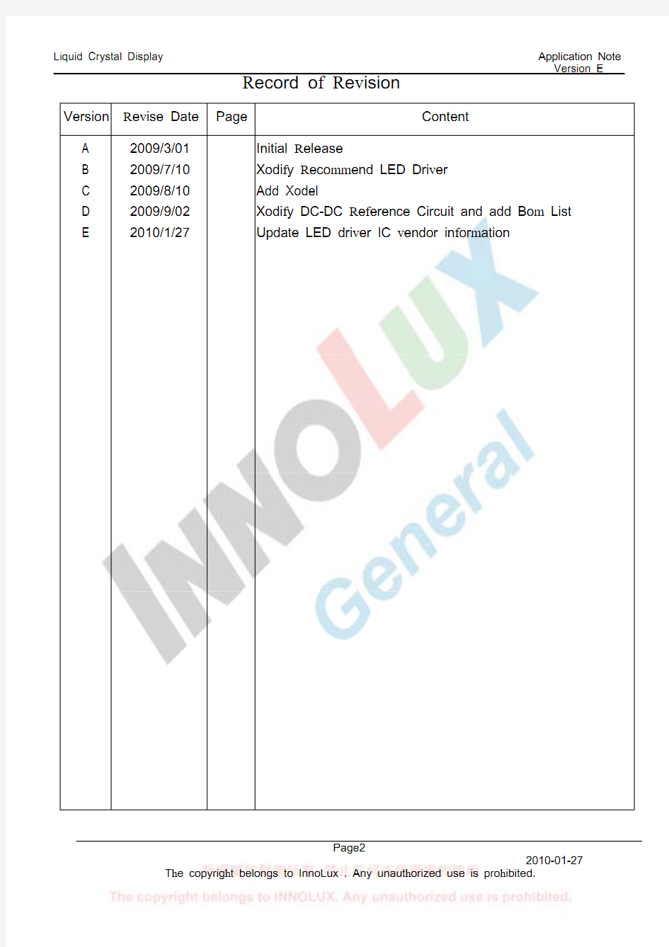
Record of Revision
Version Revise Date Page Content
A
B
C
D
E
2009/3/01
2009/7/10
2009/8/10
2009/9/02
2010/1/27
Initial Release
Modify Recommend LED Driver
Add Model
Modify DC-DC Reference Circuit and add Bom List
Update LED driver IC vendor information
1. Module Introduction
1.1 Module Photo
Module photo
Model
Top side Bottom side
AT070TN92
AT070TN93
AT070TN94
AT070TN93 V.2
1.2 Module Comparison Table
Module name Brightness(nits) Pin Num. Recommended connector AT070TN92 250(without TP) 50 pin FH12A-50S-0.5SH AT070TN93 320(with TP) 50pin FH12A-50S-0.5SH AT070TN94 400(without TP) 50 pin FH12A-50S-0.5SH
2. Pin Assignment Table
AT070TN92 &AT070TN94
Pin No.
Symbol
Pin No. Symbol I/O Function Remark
1 V LED+P Power for LED backlight (Anode)
2 V LED+P Power for LED backlight (Anode)
3 V LED-P Power for LED backlight (Cathode)
4 V LED-P Power for LED backlight (Cathode)
5 GND P Power ground
6 V COM I Common voltage
7 DV DD P Power for Digital Circuit
8 MODE I DE/SYNC mode select Note 1
9 DE I Data Input Enable
10 VS I Vertical Sync Input
11 HS I Horizontal Sync Input
12 B7 I Blue data(MSB)
13 B6 I Blue data
14 B5 I Blue data
15 B4 I Blue data
16 B3 I Blue data
17 B2 I Blue data
18 B1 I Blue data Note 2
19 B0 I Blue data(LSB) Note 2
20 G7 I Green data(MSB)
21 G6 I Green data
22 G5 I Green data
23 G4 I Green data
24 G3 I Green data
25 G2 I Green data
26 G1 I Green data Note 2
27 G0 I Green data(LSB) Note 2
28 R7 I Red data(MSB)
29 R6 I Red data
30 R5 I Red data
31 R4 I Red data
32 R3 I Red data
33 R2 I Red data
34 R1 I Red data Note 2
35 R0 I Red data(LSB) Note 2
36 GND P Power Ground
37 DCLK I Sample clock Note 3
38 GND P Power Ground
39 L/R I Left / right selection Note 4
40 U/D I Up/down selection Note 4
41 V GH P Gate ON Voltage
42 V GL P Gate OFF Voltage
43 AV DD P Power for Analog Circuit
44 RESET I Global reset pin. Noet5
45 NC - No connection
46 V COM I Common Voltage
47 DITHB I Dithering function Noet6
48 GND P Power Ground
49 NC - No connection
50 NC - No connection
I: input, O: output, P: Power
Note 1: DE/SYNC mode select. Normally pull high.
When select DE mode, MODE=”1”, VS and HS must pull high.
When select SYNC mode, MODE=”0”, DE must be grounded.
Note 2: When input 18 bits RGB data, the two low bits of R,G and B data must be grounded Note 3: Data shall be latched at the falling edge of DCLK.
Note 4: Selection of scanning mode
Setting of scan control input
Scanning direction
U/D L/R
GND DV DD Up to down, left to right
DV DD GND Down to up, right to left
GND GND Up to down, right to left
DV DD DV DD Down to up, left to right
Note 5: Global reset pin. Active low to enter reset state. Suggest to connect with an RC reset circuit for stability. Normally pull high
Note 6: Dithering function enable control, normally pull high.
When RGB is 6 bit DITHB=”1”,Disable internal dithering function,
When RGB is 8 bit DITHB=”0”,Enable internal dithering function,
3. Power &Timing Characteristic
3.1. Power Sequence
Customer should follow our product power sequence, other it would lead to display abnormal, please refer to the figures as below.
3.1.1AT070TN92 & AT070TN94
Power On:
Power Off :
Note 1: Be sure to apply DV DD and V GL to the LCD first, and then apply V GH.
Note 2: DV DD setting should match the signals output voltage (refer to Note 3) of customer’s system board.
Note 3: DCLK,HS,VS,RESET,U/D, L/R,DE,R0~R7,G0~G7,B0~B7,MODE,DITHB.
3.3 Timing Description
Input signals must follow our timing specification, Otherwise the LCM will display abnor mally.
About the detail timing parameters of LCD display, please follow the product specification.
3.3.1AC Electrical Characteristics
Values
Item Symbol
Min. Typ. Max.
Unit Remark
HS setup time Thst8 - - ns
HS hold time Thhd 8 - - ns
VS setup time Tvst8 - - ns
VS hold time Tvhd8 - - ns
Data setup time Tdsu8 - - ns
Data hole time Tdhd8 - - ns
DE setup time Tesu 8 - - ns
DE hole time Tehd8 - - ns
DV DD Power On Slew rate TPOR - - 20 ms From 0 to 90% DV DD
RESET pulse width TRst 1 - - ms DCLK cycle time Tcoh 20 - - ns DCLK pulse duty Tcwh 40 50 60 %
Timing Formula:
DCLK = (Hw + Hbp + Ha +Hfp)*( Vw + Vbp + Va +Vfp)*Fvsync (Unit : Hz) Fhsync = (Vw+ Vbp + Va +Vfp)*Fvsync (Unit : Hz)
Remark:
1. Fhsync is Hsync frequency, and Fvsync is Vsync frequency.
2. Parameter Table.
Parameter Description Unit Hw Hsync Width DCLK
Hbp Horizontal back porch DCLK
Ha Horizontal valid area DCLK
Hfp Horizontal front porch DCLK
Vw Vsync Width Hsync(Line)
Vbp Vertical back porch Hsync(Line)
Va Vertical valid area Hsync(Line)
Vfp Vertical front porch Hsync(Line)
DCLK Dot clock Hz
3.3.2Timing Chart
4. Software Introduction
NA
5. Reference Circuit
5.1 Interface reference circuit
GND R6RN1
22?1
2345678
GND R6AVDD
B4
GND B06G01B3G4
G06B0R06R02G0GND G1R7R0VGH
connector
123456789101112131415161718192021222324252627282930313233343536373839404142434445
464748
4950
VLED VLED GLED GLED GND VCOM VCC MODE DE VS HS B7B6B5B4B3B2B1B0G7G6G5G4G3G2G1G0R7R6R5R4R3R2R1R0GND DCLK GND L/R U/D VGH VGL AVDD RESET NC VCOM DITHB GND NC NC B5B3GND
G2R2VLED GLED B4G5DE B2R5R1G05G2B02R5R04
R2R1RN5
22?12345678
B6B00
G02G3GND
GLED R3DITHB G07C2?VCOM B6R07G6R4G6B1RN3
22?12345678
R3R03U/D
B0
VGH
B7RN6
22?1
2345678
VLED R00
G3MODE B7G1VS G7G00
R05RN4
22?1
2345678
G4B1B03DCLK R4R01B05B04
C1?
L/R
VCOM HS RESET
B07VCC RN2
22?12345678
G03B5B01G04
G0
G5G7R0
CLK L1
Bead 1
2
R7B2
5.2 Vcom Reference Circuit
R366.8K?
R3118K?
12
AVDDF
A V D D F
C28VCOM
VR1VR103G
R34000
C2710uF
5.3 Backlight Driver Reference Circuit
5.4 DC/DC Reference Circuit
VGH
4.7K
U101
FP6791
1
2
3
4
5678
C
C
F
B
C
S
P
V
I
N
E
X
T
V
S
S
R
O
S
C
R
D
u
t
y
10.4V
1
R133
330
1
A
V
D
D
C108
@105
C152@474
C115
@474
DM102
DAN217U
1
2
3
1
2
3
C154
@105
Rv d2
36Kohm
Rgl3
10Kohm
R123
000
C135
@105
L101
AHPD12H4R7MT
12
Q103
3904
R120
200K
3904
VGL=-7V--->
Rgl1=1K
Rgl2=430ohm
Rgl3=10K
R126
204
Q105
3906
C111
10uF
AVDDF
D103
UDZ5.6B
1
2
C110
1uF
AVDD=10.4V --->
Rvd1=39.2K
Rvd2=36k
Rvd3=2K
DAN217U
1
2
3
1
2
3
C122
10uF
Rgl2
430ohm
Rgl1
1Kohm
VGH=16V --->
Rgh1=5.1K
Rgh2=2.94K
Rgh3=5.1K
C112
@105
C106@4742
C128
@104
C114
10uF
Rgh3
5.1Kohm
D101
UDZ5.6B
1
2
C133OPEN
Rgh1
5.1Kohm
C125
@106
R125
204
1
Rgh2
2.94Kohm
C153
@105
3
3
Q106
3906
R157
102
3
C151
@105
R107
102
(0-VGL) / (Rgl1+Rgl2+Rgl3)=(0-Vref) / Rgl3
Vref=-6.3V=-5.6+(-0.7)
VGL=(Rgl1+Rgl2+Rgl3)*Vref / Rgl3
C113
@105
3
AVDD=(Rvd1//Rvd2+Rvd3)*Vref / Rvd3
Vref = 1V for FP6791
R106
103
1
R158
103
C119
OPEN
AVDD
VCC33
C121
@104
R172open
D102
SB07-03C
12
2
-7.0V
R109
474
G
N
D
DM103
DAN217U
1
2
3
1
2
3
VGH / (Rgh1+Rgh2+Rgh3) = Vref/Rgh3
VGH=(Rgh1+Rgh2+Rgh3)*Vref/Rgh3
Vref=5.6+0.7=6.3V
SW
16.0V
Rv d1
39.2Kohm
2
R121
698ohm
C131
82nF
G
N
D
2
Q104
FDN335N
3
1
2
DM104
DAN217U
1
2
3
1
2
3
Rv d3
2Kohm
Item Quantity Reference Description
1 1 U101 PWM IC FP6791,8 PIN TSSOP, Fitipower
2 4
DM101,DM102,
DM103,DM104
Diode module DAN217U, Rohm
3 2 Q102,Q103 TRANSISTOR(NPN) ,MMST3904,SC-59,Rohm
4 2 Q105,Q106 TRANSISTOR(PNP) ,MMST3906,SC-59,ROHM
5 1 Q104 MOSFET N-channel,FDN335N,SOT-23,Fairchild
6 2 D101,D103 Zener Diode,UDZ5.6B,SOD-323.Rohm
7 1 D102 SCHOTTKY BARRIER DIODE.SB07-03C, Sanyo 5.5 Vendor Recommend
Item Vendor Type Remark
DC/DC Fiti Power FP6791
LED Driver Fiti Power FP6745 1.PWM Frequency:100Hz~50KHz
2.Or other IC with the same function
6.Suggestions for housing design.
7. Demo Board Introduce
7.1 Interface of Demo Board
Connector I/O Function
1 O 5.6”D connector
2 I The hand-off controller of CVBS and D-Sub
3 P 12V DC input
4 I DVI signal input
5 I VGA signal input
6 I S-video
7 I CVBS
7.2 Interface of Remote Control
Power On/Off
Change Signal
OSD Menu
7.3 Linking LCM
关务基础知识培训题库(120109版)问题详解版
吉时关务外包基础知识培训题库JiShi Customs Outsourcing Basics Training Materials 编者:以兵 编制日期:2011-11-29
目录 练习一企业文化与规章制度 (3) 练习二 WMS系统货主与项目基础知识 (7) 练习三空运进口操作流程 (13) 练习四空运出口操作流程 (17) 练习五特殊监管区进出口操作流程 (20) 练习六海运、陆运进出口操作流程 (22) 练习七叠加保税业务进出口操作流程 (25) 练习八货代费用组成知识 (29) 练习九分送集报作业流程 (29) 综合题(一)A、B卷 综合题(二)A、B卷 综合题(三)A、B卷 综合题(四)A、B卷 综合题(五)A、B卷
练习题(企业文化与规章制度) 学员工号:学员:成绩: 一、单项选择题:(请将选择项填以下相应空格,30分) 1、以下不属于关务外包主营业务类型的是() A、关务诊断 B、关务咨询 C、关务招聘 D、关务操作 2、关务外包倡导的企业文化精神是()。 A、专业敬业诚信共赢 B、专业守业诚信共赢 C、清洁清扫整理整顿 D、清洁清扫整理素养 3、物流园按照进出口业务类型来分,以下不属于此类分类的是() A、空运进出口 B、仓库收出货业务 C、特殊监管区进出口 D、叠加进出口 4、以下关于年假说确的是(B) A、本年度未使用完的年假,可累计到下年度使用 B、年假是可分批次使用 C、为公司服务满6个会计年度的员工享有5天的年假 D、本年度病事假累计超过10天不享受年假 5、以下说法错误的是(B) A、符合国家法定年龄结婚的员工享受3天带薪婚假 B、晚婚(女满24周岁,男满25周岁),带薪婚假10天 C、婚假是一次性安排领取结婚证为标准 D、婚假以领取结婚证为标准 6、请假注意事项正确的是(B) A、请假可直接填写请假卡,再由领导签字确认 B、请假情况以形式告知部门助理 C、未请假或未续假,可有补假 D、上班时间可外出办理个人私事 7、关于部门车辆使用情况,正确的是(A) A、因关务外包部或客服部、企业事务需要外出,申请使用车辆 B、出车前填写派车单,经理或主管签字后,司机凭派车单外出 C、出车后应按照派车单上的地点和时间进行,可拖延时间 D、如车辆使用紧凑,根据派车单的填写顺序安排
关务水平考试
附件1 2018年关务水平测试大纲 说明 关务水平测试是对参测人员关务基础知识与关务基本技能进行的职业能力测试,是中国报关协会依据我国海关法律法规和《报关服务作业规范》、《报关服务质量要求》等行业标准,结合行业发展需求建立的关务水平评价体系的组成部分。 关务水平测试在内容上以企业需求和就业为设计导向,以考察专业知识和岗位实操技能为测试目标。通过客观、公平、科学、系统的多维评测,关务水平测试可以为企业选聘专业人才和院校专业人才培养提供客观的标准和依据。 中国报关协会组织行业内专家、学者集体编写关务水平测试大纲,力求较为全面反映关务从业人员的基本业务知识和业务技能要求,尽可能体现海关业务改革和行业发展的最新成果。 关务水平测试大纲每年与考试公告同时向社会公布。 科目一关务基础知识 一、对外贸易 (一)主要内容 n对外贸易的含义、特点、分类、方式和基本业务程序; n进出口合同的格式和主要条款; n进出口商品品质、数量、包装的基础知识;
n国际贸易术语的基础知识; n进出口货物运输与保险的基础知识; n对外贸易结算工具与方式的基础知识。 (二)基本要求 n理解对外贸易的基本特点、类型及涉及的业务范围; n熟悉对外贸易的交易方式; n掌握国际货物买卖的不同交易方式与海关监管方式的关系; n熟悉对外贸易的业务各环节的基本程序; n掌握履行进出口贸易合同阶段的收发货、通关环节的报关、报验作业的节点; n理解进出口合同的结构、内容、生效的条件及法律的适用; n熟悉进出口合同各条款的基本内容; n掌握当事人履约过程各环节所涉及的不同业务领域及应办理的事务; n理解履约过程中当事人的责任、权利、义务及国际惯例; n掌握货物进出口业务中各类事务处置的基本规则; n熟悉制定进出口合同品质条款所涉及的相关商品知识、规定方式、违约责任; n掌握合同交易标的的品质,确定归类对象的商品属性; n熟悉进出口合同对商品的数量、机动幅度、违约责任规定的具体方式和要求;