MAX3232EETE中文资料

General Description
The MAX3222E/MAX3232E/MAX3237E/MAX3241E/MAX3246E +3.0V-powered EIA/TIA-232 and V.28/V.24communications interface devices feature low power con-sumption, high data-rate capabilities, and enhanced electrostatic-discharge (ESD) protection. The enhanced ESD structure protects all transmitter outputs and receiver inputs to ±15kV using IEC 1000-4-2 Air-G ap Discharge, ±8kV using IEC 1000-4-2 Contact Discharge (±9kV for MAX3246E), and ±15kV using the Human Body Model. The logic and receiver I/O pins of the MAX3237E are protected to the above standards, while the transmit-ter output pins are protected to ±15kV using the Human Body Model.
A proprietary low-dropout transmitter output stage delivers true RS-232 performance from a +3.0V to +5.5V power supply, using an internal dual charge pump. The charge pump requires only four small 0.1μF capacitors for opera-tion from a +3.3V supply. Each device guarantees opera-tion at data rates of 250kbps while maintaining RS-232output levels. The MAX3237E guarantees operation at 250kbps in the normal operating mode and 1Mbps in the MegaBaud? operating mode, while maintaining RS-232-compliant output levels.
The MAX3222E/MAX3232E have two receivers and two transmitters. The MAX3222E features a 1μA shutdown mode that reduces power consumption in battery-pow-ered portable systems. The MAX3222E receivers remain active in shutdown mode, allowing monitoring of external devices while consuming only 1μA of supply current. The MAX3222E and MAX3232E are pin, package, and func-tionally compatible with the industry-standard MAX242and MAX232, respectively.
The MAX3241E/MAX3246E are complete serial ports (three drivers/five receivers) designed for notebook and subnotebook computers. The MAX3237E (five drivers/three receivers) is ideal for peripheral applications that require fast data transfer. These devices feature a shut-down mode in which all receivers remain active, while consuming only 1μA (MAX3241E/MAX3246E) or 10nA (MAX3237E).
The MAX3222E, MAX3232E, and MAX3241E are avail-able in space-saving SO, SSOP, TQFN and TSSOP pack-ages. The MAX3237E is offered in an SSOP package.The MAX3246E is offered in the ultra-small 6 x 6 UCSP?package.
Applications
Battery-Powered Equipment Printers
Cell Phones
Smart Phones Cell-Phone Data Cables xDSL Modems
Notebook, Subnotebook,and Palmtop Computers
Next-Generation Device Features
?For Space-Constrained Applications
MAX3228E/MAX3229E: ±15kV ESD-Protected, +2.5V to +5.5V, RS-232 Transceivers in UCSP ?For Low-Voltage or Data Cable Applications
MAX3380E/MAX3381E: +2.35V to +5.5V, 1μA, 2Tx/2Rx, RS-232 Transceivers with ±15kV ESD-Protected I/O and Logic Pins
MAX3222E/MAX3232E/MAX3237E/MAX3241E ?/MAX3246E
±15kV ESD-Protected, Down to 10nA, 3.0V to 5.5V ,
Up to 1Mbps, True RS-232 Transceivers
________________________________________________________________Maxim Integrated Products 1
19-1298; Rev 10; 1/06
Ordering Information continued at end of data sheet.*Dice are tested at T A = +25°C, DC parameters only.**EP = Exposed paddle.
Pin Configurations, Selector Guide, and Typical Operating Circuits appear at end of data sheet.
For pricing, delivery, and ordering information,please contact Maxim/Dallas Direct!at 1-888-629-4642, or visit Maxim’s website at https://www.sodocs.net/doc/3816481328.html,.
MegaBaud and UCSP are trademarks of Maxim Integrated Products, Inc.
?Covered by U.S. Patent numbers 4,636,930; 4,679,134;
4,777,577; 4,797,899; 4,809,152; 4,897,774; 4,999,761; and other patents pending.
M A X 3222E /M A X 3232E /M A X 3237E /M A X 3241E ?/M A X 3246E
±15kV ESD-Protected, Down to 10nA, 3.0V to 5.5V ,Up to 1Mbps, True RS-232 Transceivers
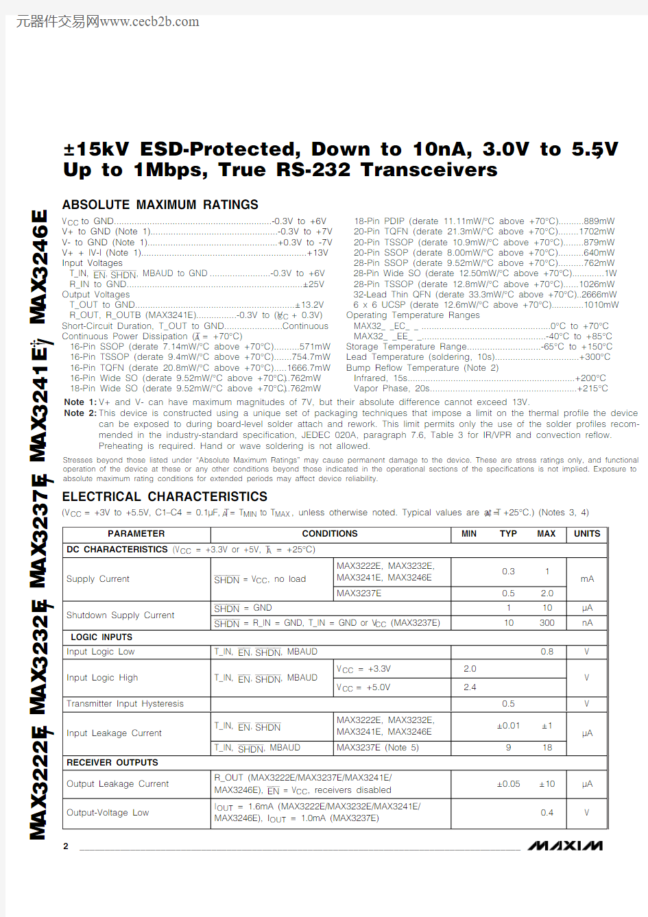
ABSOLUTE MAXIMUM RATINGS
ELECTRICAL CHARACTERISTICS
(V CC = +3V to +5.5V, C1–C4 = 0.1μF, T A = T MIN to T MAX , unless otherwise noted. Typical values are at T A = +25°C.) (Notes 3, 4)
Stresses beyond those listed under “Absolute Maximum Ratings” may cause permanent damage to the device. These are stress ratings only, and functional operation of the device at these or any other conditions beyond those indicated in the operational sections of the specifications is not implied. Exposure to absolute maximum rating conditions for extended periods may affect device reliability.
V CC to GND..............................................................-0.3V to +6V V+ to GND (Note 1)..................................................-0.3V to +7V V- to GND (Note 1)...................................................+0.3V to -7V V+ + |V-| (Note 1).................................................................+13V Input Voltages T_IN, EN , SHDN , MBAUD to GND ........................-0.3V to +6V R_IN to GND.....................................................................±25V Output Voltages T_OUT to GND...............................................................±13.2V R_OUT, R_OUTB (MAX3241E)................-0.3V to (V CC + 0.3V)Short-Circuit Duration, T_OUT to GND.......................Continuous Continuous Power Dissipation (T A = +70°C)16-Pin SSOP (derate 7.14mW/°C above +70°C)..........571mW 16-Pin TSSOP (derate 9.4mW/°C above +70°C).......754.7mW 16-Pin TQFN (derate 20.8mW/°C above +70°C).....1666.7mW 16-Pin Wide SO (derate 9.52mW/°C above +70°C).....762mW 18-Pin Wide SO (derate 9.52mW/°C above +70°C).....762mW 18-Pin PDIP (derate 11.11mW/°C above +70°C)..........889mW 20-Pin TQFN (derate 21.3mW/°C above +70°C)........1702mW 20-Pin TSSOP (derate 10.9mW/°C above +70°C)........879mW 20-Pin SSOP (derate 8.00mW/°C above +70°C)..........640mW 28-Pin SSOP (derate 9.52mW/°C above +70°C)..........762mW 28-Pin Wide SO (derate 12.50mW/°C above +70°C).............1W 28-Pin TSSOP (derate 12.8mW/°C above +70°C)......1026mW 32-Lead Thin QFN (derate 33.3mW/°C above +70°C)..2666mW 6 x 6 UCSP (derate 12.6mW/°C above +70°C).............1010mW Operating Temperature Ranges MAX32_ _EC_ _...................................................0°C to +70°C MAX32_ _EE_ _.................................................-40°C to +85°C Storage Temperature Range.............................-65°C to +150°C Lead Temperature (soldering, 10s).................................+300°C Bump Reflow Temperature (Note 2)Infrared, 15s..................................................................+200°C Vapor Phase, 20s..........................................................+215°C Note 1:V+ and V- can have maximum magnitudes of 7V, but their absolute difference cannot exceed 13V.
Note 2:This device is constructed using a unique set of packaging techniques that impose a limit on the thermal profile the device
can be exposed to during board-level solder attach and rework. This limit permits only the use of the solder profiles recom-mended in the industry-standard specification, JEDEC 020A, paragraph 7.6, Table 3 for IR/VPR and convection reflow.Preheating is required. Hand or wave soldering is not allowed.
MAX3222E/MAX3232E/MAX3237E/MAX3241E ?/MAX3246E
±15kV ESD-Protected, Down to 10nA, 3.0V to 5.5V ,
Up to 1Mbps, True RS-232 Transceivers
_______________________________________________________________________________________3
M A X 3222E /M A X 3232E /M A X 3237E /M A X 3241E ?/M A X 3246E
±15kV ESD-Protected, Down to 10nA, 3.0V to 5.5V ,Up to 1Mbps, True RS-232 Transceivers
4_______________________________________________________________________________________
TIMING CHARACTERISTICS—MAX3237E
(V CC = +3V to +5.5V, C1–C4 = 0.1μF, T A = T MIN to T MAX , unless otherwise noted. Typical values are at T A = +25°C.) (Note 3)
±10%. MAX3237E: C1–C4 = 0.1μF tested at +3.3V ±5%, C1–C4 = 0.22μF tested at +3.3V ±10%; C1 = 0.047μF, C2, C3, C4 =0.33μF tested at +5.0V ±10%. MAX3246E; C1-C4 = 0.22μF tested at +3.3V ±10%; C1 = 0.22μF, C2, C3, C4 = 0.54μF tested at 5.0V ±10%.
Note 4:MAX3246E devices are production tested at +25°C. All limits are guaranteed by design over the operating temperature range.Note 5:The MAX3237E logic inputs have an active positive feedback resistor. The input current goes to zero when the inputs are at
the supply rails.
Note 6:MAX3241EEUI is specified at T A = +25°C.
Note 7:Transmitter skew is measured at the transmitter zero crosspoints.
TIMING CHARACTERISTICS—MAX3222E/MAX3232E/MAX3241E/MAX3246E
MAX3222E/MAX3232E/MAX3237E/MAX3241E ?/MAX3246E
±15kV ESD-Protected, Down to 10nA, 3.0V to 5.5V ,
Up to 1Mbps, True RS-232 Transceivers
_______________________________________________________________________________________
5
-6
-4-202460
MAX3237E
TRANSMITTER OUTPUT VOLTAGE vs. LOAD CAPACITANCE (MBAUD = GND)
LOAD CAPACITANCE (pF)
T R A N S M I T T E R O U T P U T V O L T A G E (V )
1000
1500
500
2000
2500
3000
531-1-3-5-6
-2-42046-5-31-1350
1000
1500
500
2000
2500
3000
LOAD CAPACITANCE (pF)T R A N S M I T T E R O U T P U T V O L T A G E (V )
MAX3237E
TRANSMITTER OUTPUT VOLTAGE
vs. LOAD CAPACITANCE
-7.5
-5.0-2.502.55.07.5
MAX3237E
TRANSMITTER OUTPUT VOLTAGE vs. LOAD CAPACITANCE (MBAUD = V CC )
LOAD CAPACITANCE (pF)
T R A N S M I T T E R O U T P U T V O L T A G E (V )
500
1000
1500
2000
__________________________________________Typical Operating Characteristics
(V CC = +3.3V, 250kbps data rate, 0.1μF capacitors, all transmitters loaded with 3k ?
and C L , T A = +25°C, unless otherwise noted.)
-6
-5-4-3-2-101234560
1000
2000
3000
4000
5000
MAX3241E
TRANSMITTER OUTPUT VOLTAGE
vs. LOAD CAPACITANCE
LOAD CAPACITANCE (pF)T R A N S M I T T E R O U T P U T V O L T A G E (
V )
30
2010405060020001000300040005000
MAX3241E
OPERATING SUPPLY CURRENT vs. LOAD CAPACITANCE
LOAD CAPACITANCE (pF)
S U P P L Y C U R R E N T (m A )
04
2861210140
1000
2000
3000
4000
5000
MAX3241E
SLEW RATE vs. LOAD CAPACITANCE
M A X 3237E t o c 05
LOAD CAPACITANCE (pF)S L E W R A T E (V /μ
s )
-6
-5-4-3-2-101234560
1000
2000
3000
4000
5000
MAX3222E/MAX3232E
TRANSMITTER OUTPUT VOLTAGE
vs. LOAD CAPACITANCE
LOAD CAPACITANCE (pF)T R A N S M I T T E R O U T P U T
V O L T A G E (V )
62
4
1081412160
1000
2000
3000
4000
5000
MAX3222E/MAX3232E
SLEW RATE vs. LOAD CAPACITANCE
LOAD CAPACITANCE (pF)S L E W R A T E (V /μs
)
252015510
35304045
2000
1000
3000
4000
5000
MAX3222E/MAX3232E OPERATING SUPPLY CURRENT vs. LOAD CAPACITANCE
LOAD CAPACITANCE (pF)
S U P P L Y C U R R E N T (m A )
M A X 3222E /M A X 3232E /M A X 3237E /M A X 3241E ?/M A X 3246E
±15kV ESD-Protected, Down to 10nA, 3.0V to 5.5V ,Up to 1Mbps, True RS-232 Transceivers
6_______________________________________________________________________________________
Typical Operating Characteristics (continued)
(V CC = +3.3V, 250kbps data rate, 0.1μF capacitors, all transmitters loaded with 3k ?and C L , T A = +25°C, unless otherwise noted.)
20
6040
80
100
MAX3237E
TRANSMITTER SKEW vs. LOAD CAPACITANCE
(MBAUD = V CC )
LOAD CAPACITANCE (pF)
1000
1500
500
2000
T R A N S M I T T E R S K E W (n s )
-6
-2-42046-3-51-1352.0
3.0
3.5
2.5
4.0
4.5
5.0
SUPPLY VOLTAGE (V)
T R A N S M I T T E R O U T P U T V O L T A G E (V )
MAX3237E
TRANSMITTER OUTPUT VOLTAGE vs. SUPPLY VOLTAGE (MBAUD = GND)
10
2030
4050
2.0
MAX3237E SUPPLY CURRENT vs. SUPPLY VOLTAGE (MBAUD = GND)
SUPPLY VOLTAGE (V)
S U P P L Y C U R R E N T (m A )
3.0
3.5
2.5
4.0
4.5
5.0
MAX3246E
TRANSMITTER OUTPUT VOLTAGE
vs. LOAD CAPACITANCE
LOAD CAPACITANCE (pF)
T R A N S M I T T E R O U T P U T V O L T A G E (V )
4000
3000
1000
2000
-5-4-3-2-101234567-6
5000
4
6
810
1214160
MAX3246E
SLEW RATE vs. LOAD CAPACITANCE
LOAD CAPACITANCE (pF)
S L E W
R A T E (V /μs )
2000
3000
1000
4000
5000
102030405060
0MAX3246E
OPERATING SUPPLY CURRENT vs. LOAD CAPACITANCE
M A X 3237E t o c 17
LOAD CAPACITANCE (pF)
S U P P L Y C U R R E
N T (m A )
10002000300040005000
5545352515502468
10
12
MAX3237E
SLEW RATE vs. LOAD CAPACITANCE
(MBAUD = GND)
LOAD CAPACITANCE (pF)S L E W R A T E (V /μs )
1000
1500
500
2000
2500
30000
10203050406070
MAX3237E
SLEW RATE vs. LOAD CAPACITANCE
(MBAUD = V CC )
LOAD CAPACITANCE (pF)
S L E W R A T E (V /μs )
500
1000
1500
2000
10
20
30
4050
MAX3237E
SUPPLY CURRENT vs. LOAD CAPACITANCE WHEN TRANSMITTING DATA (MBAUD = GND)
LOAD CAPACITANCE (pF)
S U P P L Y C U R R E N T (m A )
1000
1500
500
2000
2500
3000
MAX3222E/MAX3232E/MAX3237E/MAX3241E ?/MAX3246E
±15kV ESD-Protected, Down to 10nA, 3.0V to 5.5V ,
Up to 1Mbps, True RS-232 Transceivers
_______________________________________________________________________________________7
Pin Description
M A X 3222E /M A X 3232E /M A X 3237E /M A X 3241E ?/M A X 3246E
±15kV ESD-Protected, Down to 10nA, 3.0V to 5.5V ,Up to 1Mbps, True RS-232 Transceivers
8_______________________________________________________________________________________
MAX3222E/MAX3232E/MAX3237E/MAX3241E ?/MAX3246E
±15kV ESD-Protected, Down to 10nA, 3.0V to 5.5V ,
Up to 1Mbps, True RS-232 Transceivers
_______________________________________________________________________________________9
Detailed Description
Dual Charge-Pump Voltage Converter
The MAX3222E/MAX3232E/MAX3237E/MAX3241E/MAX3246Es’ internal power supply consists of a regu-lated dual charge pump that provides output voltages of +5.5V (doubling charge pump) and -5.5V (inverting charge pump) over the +3.0V to +5.5V V CC range. The charge pump operates in discontinuous mode; if the output voltages are less than 5.5V, the charge pump is enabled, and if the output voltages exceed 5.5V, the charge pump is disabled. Each charge pump requires a flying capacitor (C1, C2) and a reservoir capacitor (C3, C4) to generate the V+ and V- supplies (Figure 1).
RS-232 Transmitters
The transmitters are inverting level translators that con-vert TTL/CMOS-logic levels to ±5V EIA/TIA-232-compli-ant levels.
The MAX3222E/MAX3232E/MAX3237E/MAX3241E/MAX3246E transmitters guarantee a 250kbps data rate with worst-case loads of 3k ?in parallel with 1000pF,providing compatibility with PC-to-PC communication software (such as LapLink?). Transmitters can be par-alleled to drive multiple receivers or mice.
The MAX3222E/MAX3237E/MAX3241E/MAX3246E transmitters are disabled and the outputs are forced
into a high-impedance state when the device is in shut-down mode (SHDN = G ND). The MAX3222E/MAX3232E/MAX3237E/MAX3241E/MAX3246E permit the outputs to be driven up to ±12V in shutdown.
The MAX3222E/MAX3232E/MAX3241E/MAX3246E transmitter inputs do not have pullup resistors. Connect unused inputs to GND or V CC . The MAX3237E’s trans-mitter inputs have a 400k ?active positive-feedback resistor, allowing unused inputs to be left unconnected.
MAX3237E MegaBaud Operation
For higher-speed serial communications, the MAX3237E features MegaBaud operation. In MegaBaud operating mode (MBAUD = V CC ), the MAX3237E transmitters guarantee a 1Mbps data rate with worst-case loads of 3k ?in parallel with 250pF for +3.0V < V CC < +4.5V. For +5V ±10% operation, the MAX3237E transmitters guarantee a 1Mbps data rate into worst-case loads of 3k ?in parallel with 1000pF.
RS-232 Receivers
The receivers convert RS-232 signals to CMOS-logic output levels. The MAX3222E/MAX3237E/MAX3241E/MAX3246E receivers have inverting three-state outputs.Drive EN high to place the receiver(s) into a high-impedance state. Receivers can be either active or inactive in shutdown (Table 1).
Figure 1. Slew-Rate Test Circuits
LapLink is a trademark of Traveling Software.
M A X 3222E /M A X 3232E /M A X 3237E /M A X 3241E ?/M A X 3246E
±15kV ESD-Protected, Down to 10nA, 3.0V to 5.5V ,Up to 1Mbps, True RS-232 Transceivers
10
______________________________________________________________________________________
The complementary outputs on the MAX3237E/MAX3241E (R_OUTB) are always active, regardless of the state of EN or SHDN . This allows the device to be used for ring indicator applications without forward biasing other devices connected to the receiver outputs. This is ideal for systems where V CC drops to zero in shutdown to accommodate peripherals such as UARTs (Figure 2).
MAX3222E/MAX3237E/MAX3241E/
MAX3246E Shutdown Mode
Supply current falls to less than 1μA in shutdown mode (SHDN = low). The MAX3237E’s supply current falls to10nA (typ) when all receiver inputs are in the invalid range (-0.3V < R_IN < +0.3). When shut down, the device’s charge pumps are shut off, V+ is pulled down to V CC , V- is pulled to ground, and the transmitter out-puts are disabled (high impedance). The time required to recover from shutdown is typically 100μs, as shown in Figure 3. Connect SHDN to V CC if shutdown mode is not used. SHDN has no effect on R_OUT or R_OUTB (MAX3237E/MAX3241E).
±15kV ESD Protection
As with all Maxim devices, ESD-protection structures are incorporated to protect against electrostatic dis-charges encountered during handling and assembly.The driver outputs and receiver inputs of the MAX3222E/MAX3232E/MAX3237E/MAX3241E/MAX3246E have extra protection against static electricity. Maxim’s engineers have developed state-of-the-art structures to protect these pins against ESD of ±15kV without damage.The ESD structures withstand high ESD in all states:normal operation, shutdown, and powered down. After an ESD event, Maxim’s E versions keep working without latchup, whereas competing RS-232 products can latch and must be powered down to remove latchup.
Furthermore, the MAX3237E logic I/O pins also have ±15kV ESD protection. Protecting the logic I/O pins to ±15kV makes the MAX3237E ideal for data cable applications.
SHDN T2OUT
T1OUT
5V/div
2V/div
V CC = 3.3V C1–C4 = 0.1μF
Figure 3. Transmitter Outputs Recovering from Shutdown or Powering Up
MAX3222E/MAX3232E/MAX3237E/MAX3241E ?/MAX3246E
±15kV ESD-Protected, Down to 10nA, 3.0V to 5.5V ,
Up to 1Mbps, True RS-232 Transceivers
______________________________________________________________________________________
11
ESD protection can be tested in various ways; the transmitter outputs and receiver inputs for the MAX3222E/MAX3232E/MAX3241E/MAX3246E are characterized for protection to the following limits:?±15kV using the Human Body Model
?±8kV using the Contact Discharge method specified in IEC 1000-4-2
?±9kV (MAX3246E only) using the Contact Discharge method specified in IEC 1000-4-2
?±15kV using the Air-G ap Discharge method speci-
fied in IEC 1000-4-2
Figure 4a. Human Body ESD Test Model
Figure 4b. Human Body Model Current Waveform
Figure 5a. IEC 1000-4-2 ESD Test Model Figure 5b. IEC 1000-4-2 ESD Generator Current Waveform
M A X 3222E /M A X 3232E /M A X 3237E /M A X 3241E ?/M A X 3246E
±15kV ESD-Protected, Down to 10nA, 3.0V to 5.5V ,Up to 1Mbps, True RS-232 Transceivers
12
______________________________________________________________________________________
characterized for protection to ±15kV per the Human Body Model.
ESD Test Conditions
ESD performance depends on a variety of conditions.Contact Maxim for a reliability report that documents test setup, test methodology, and test results.
Human Body Model
Figure 4a shows the Human Body Model, and Figure 4b shows the current waveform it generates when dis-charged into a low impedance. This model consists of a 100pF capacitor charged to the ESD voltage of interest,which is then discharged into the test device through a 1.5k ?resistor.
IEC 1000-4-2
The IEC 1000-4-2 standard covers ESD testing and performance of finished equipment; it does not specifi-cally refer to integrated circuits. The MAX3222E/MAX3232E/MAX3237E/MAX3241E/MAX3246E help you design equipment that meets level 4 (the highest level)of IEC 1000-4-2, without the need for additional ESD-protection components.
The major difference between tests done using the Human Body Model and IEC 1000-4-2 is higher peak current in IEC 1000-4-2, because series resistance is lower in the IEC 1000-4-2 model. Hence, the ESD with-stand voltage measured to IEC 1000-4-2 is generally lower than that measured using the Human Body Model. Figure 5a shows the IEC 1000-4-2 model, and Figure 5b shows the current waveform for the ±8kV IEC 1000-4-2 level 4 ESD Contact Discharge test. The Air-G ap Discharge test involves approaching the device with a charged probe. The Contact Discharge method connects the probe to the device before the probe is energized.
Machine Model
The Machine Model for ESD tests all pins using a 200pF storage capacitor and zero discharge resis-tance. Its objective is to emulate the stress caused by contact that occurs with handling and assembly during manufacturing. All pins require this protection during manufacturing, not just RS-232 inputs and outputs.Therefore, after PC board assembly, the Machine Model is less relevant to I/O ports.
Table 2. Required Minimum Capacitor Values
Figure 6a. MAX3241E Transmitter Output Voltage vs. Load Current Per Transmitter
Table 3. Logic-Family Compatibility with Various Supply Voltages
MAX3222E/MAX3232E/MAX3237E/MAX3241E ?/MAX3246E
±15kV ESD-Protected, Down to 10nA, 3.0V to 5.5V ,
Up to 1Mbps, True RS-232 Transceivers
______________________________________________________________________________________13
Applications Information
Capacitor Selection
The capacitor type used for C1–C4 is not critical for proper operation; polarized or nonpolarized capacitors can be used. The charge pump requires 0.1μF capaci-tors for 3.3V operation. For other supply voltages, see Table 2 for required capacitor values. Do not use val-ues smaller than those listed in Table 2. Increasing the capacitor values (e.g., by a factor of 2) reduces ripple on the transmitter outputs and slightly reduces power consumption. C2, C3, and C4 can be increased without changing C1’s value. However, do not increase C1without also increasing the values of C2, C3, C4,and C BYPASS to maintain the proper ratios (C1 to the other capacitors).
When using the minimum required capacitor values,make sure the capacitor value does not degrade
excessively with temperature. If in doubt, use capaci-tors with a larger nominal value. The capacitor’s equiv-alent series resistance (ESR), which usually rises at low temperatures, influences the amount of ripple on V+and V-.
Power-Supply Decoupling
In most circumstances, a 0.1μF V CC bypass capacitor is adequate. In applications sensitive to power-supply noise, use a capacitor of the same value as charge-pump capacitor C1. Connect bypass capacitors as close to the IC as possible.
Operation Down to 2.7V
Transmitter outputs meet EIA/TIA-562 levels of ±3.7V with supply voltages as low as 2.7V.
Figure 6b. Mouse Driver Test Circuit
M A X 3222E /M A X 3232E /M A X 3237E /M A X 3241E ?/M A X 3246E
±15kV ESD-Protected, Down to 10nA, 3.0V to 5.5V ,Up to 1Mbps, True RS-232 Transceivers
14
______________________________________________________________________________________
Figure 7. Loopback Test Circuit
T1IN T1OUT
R1OUT
5V/div
5V/div
5V/div
V CC = 3.3V C1–C4 = 0.1μF
Figure 8. MAX3241E Loopback Test Result at 120kbps T1IN
T1OUT
R1OUT
5V/div
5V/div
5V/div
V CC = 3.3V, C1–C4 = 0.1μF
Figure 9. MAX3241E Loopback Test Result at 250kbps
+5V 0
+5V 0-5V +5V
T_IN
T_OUT
5k ? + 250pF
R_OUT
V CC = 3.3V C1–C4 = 0.1μF
Figure 10. MAX3237E Loopback Test Result at 1000kbps (MBAUD = V CC )
Transmitter Outputs Recovering
from Shutdown
Figure 3 shows two transmitter outputs recovering from shutdown mode. As they become active, the two trans-mitter outputs are shown going to opposite RS-232 levels (one transmitter input is high; the other is low). Each transmitter is loaded with 3k ?in parallel with 2500pF.The transmitter outputs display no ringing or undesir-able transients as they come out of shutdown. Note that
the transmitters are enabled only when the magnitude of V- exceeds approximately -3.0V.
Mouse Drivability
The MAX3241E is designed to power serial mice while operating from low-voltage power supplies. It has been tested with leading mouse brands from manu-facturers such as Microsoft and Logitech. The MAX3241E successfully drove all serial mice tested and met their current and voltage requirements.
MAX3222E/MAX3232E/MAX3237E/MAX3241E ?/MAX3246E
±15kV ESD-Protected, Down to 10nA, 3.0V to 5.5V ,
Up to 1Mbps, True RS-232 Transceivers
______________________________________________________________________________________15
Figure 6a shows the transmitter output voltages under increasing load current at +3.0V. Figure 6b shows a typical mouse connection using the MAX3241E.
High Data Rates
The MAX3222E/MAX3232E/MAX3237E/MAX3241E/MAX3246E maintain the RS-232 ±5V minimum transmit-ter output voltage even at high data rates. Figure 7shows a transmitter loopback test circuit. Figure 8shows a loopback test result at 120kbps, and Figure 9shows the same test at 250kbps. For Figure 8, all trans-mitters were driven simultaneously at 120kbps into RS-232 loads in parallel with 1000pF. For Figure 9, a single transmitter was driven at 250kbps, and all transmitters were loaded with an RS-232 receiver in parallel with 1000pF.
The MAX3237E maintains the RS-232 ±5.0V minimum transmitter output voltage at data rates up to 1Mbps.Figure 10 shows a loopback test result at 1Mbps with MBAUD = V CC . For Figure 10, all transmitters were loaded with an RS-232 receiver in parallel with 250pF.
Interconnection with 3V and 5V Logic
The MAX3222E/MAX3232E/MAX3237E/MAX3241E/MAX3246E can directly interface with various 5V logic families, including ACT and HCT CMOS. See Table 3for more information on possible combinations of inter-connections.
UCSP Reliability
The UCSP represents a unique packaging form factor that may not perform equally to a packaged product through traditional mechanical reliability tests. UCSP reliability is integrally linked to the user’s assembly methods, circuit board material, and usage environ-ment. The user should closely review these areas when considering use of a UCSP package. Performance through Operating Life Test and Moisture Resistance remains uncompromised as the wafer-fabrication process primarily determines it.
Mechanical stress performance is a greater considera-tion for a UCSP package. UCSPs are attached through direct solder contact to the user’s PC board, foregoing the inherent stress relief of a packaged product lead frame. Solder joint contact integrity must be consid-ered. Table 4 shows the testing done to characterize the UCSP reliability performance. In conclusion, the UCSP is capable of performing reliably through envi-ronmental stresses as indicated by the results in the table. Additional usage data and recommendations are detailed in the UCSP application note, which can be found on Maxim’s website at https://www.sodocs.net/doc/3816481328.html,.
Table 4. Reliability Test Data
M A X 3222E /M A X 3232E /M A X 3237E /M A X 3241E ?/M A X 3246E
±15kV ESD-Protected, Down to 10nA, 3.0V to 5.5V ,Up to 1Mbps, True RS-232 Transceivers
16______________________________________________________________________________________
__________________________________________________________Pin Configurations
MAX3222E/MAX3232E/MAX3237E/MAX3241E ?/MAX3246E
±15kV ESD-Protected, Down to 10nA, 3.0V to 5.5V ,
Up to 1Mbps, True RS-232 Transceivers
Pin Configurations (continued)
M A X 3222E /M A X 3232E /M A X 3237E /M A X 3241E ?/M A X 3246E
±15kV ESD-Protected, Down to 10nA, 3.0V to 5.5V ,Up to 1Mbps, True RS-232 Transceivers
18______________________________________________________________________________________
__________________________________________________Typical Operating Circuits
MAX3222E/MAX3232E/MAX3237E/MAX3241E ?/MAX3246E
±15kV ESD-Protected, Down to 10nA, 3.0V to 5.5V ,
Up to 1Mbps, True RS-232 Transceivers
______________________________________________________________________________________19
_____________________________________Typical Operating Circuits (continued)
M A X 3222E /M A X 3232E /M A X 3237E /M A X 3241E ?/M A X 3246E
±15kV ESD-Protected, Down to 10nA, 3.0V to 5.5V ,Up to 1Mbps, True RS-232 Transceivers
20______________________________________________________________________________________
_____________________________________Typical Operating Circuits (continued)