BD5325中文资料
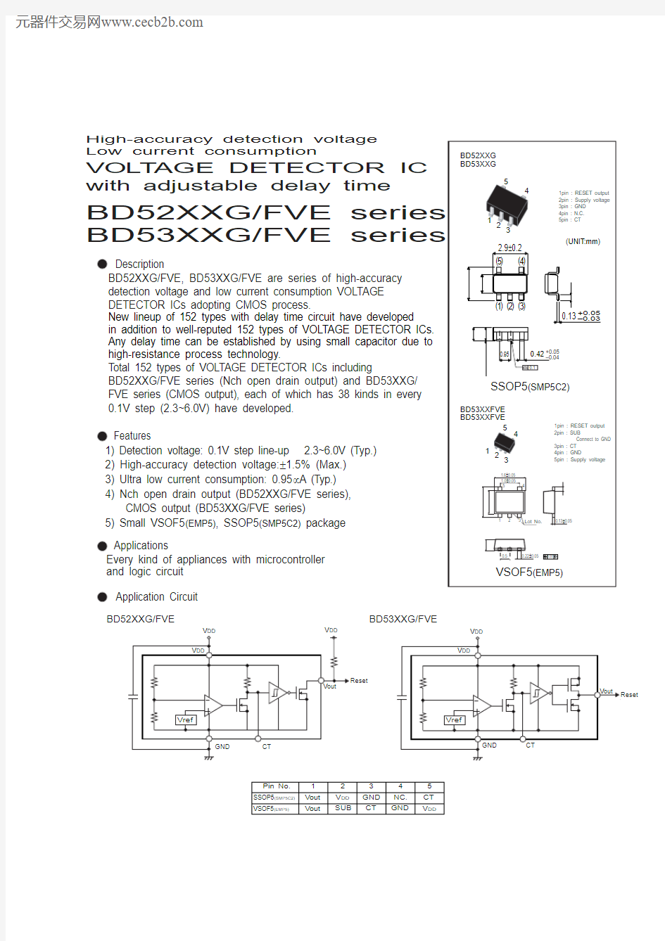

BD52XXG/FVE series BD53XXG/FVE series
High-accuracy detection voltage Low current consumption
Description
Features
Applications VOL T AGE DETECTOR IC with adjustable delay time
BD52XXG/FVE, BD53XXG/FVE are series of high-accuracy detection voltage and low current consumption VOLTAGE DETECTOR ICs adopting CMOS process.
New lineup of 152 types with delay time circuit have developed in addition to well-reputed 152 types of VOLTAGE DETECTOR ICs.Any delay time can be established by using small capacitor due to high-resistance process technology.
Total 152 types of VOLTAGE DETECTOR ICs including
BD52XXG/FVE series (Nch open drain output) and BD53XXG/FVE series (CMOS output), each of which has 38 kinds in every 0.1V step (2.3~6.0V) have developed.1) Detection voltage: 0.1V step line-up 2.3~6.0V (Typ.)2) High-accuracy detection voltage:±1.5% (Max.)3) Ultra low current consumption: 0.95μA (Typ.)4) Nch open drain output (BD52XXG/FVE series), CMOS output (BD53XXG/FVE series)
5) Small VSOF5(EMP5), SSOP5(SMP5C2) package
Every kind of appliances with microcontroller and logic circuit BD52XXG/FVE
BD53XXG/FVE
Pin No.SSOP5(SMP5C2)VSOF5(EMP5)
Vout Vout
V DD V DD
GND GND
NC.CT SUB
CT
12345 Application Circuit
Absolute Maximum Ratings (Ta=25?C)
Characteristic diagram and Measurement circuit
Electrical characteristics (Unless otherwise noted; Ta=-25~85?C)
1 ?C ?C *
2 Derating: 2.1mW/?C for operation above Ta=25?C .(Mounted on a 70.0mmX70.0mmX16mm glass epoxy PCB.)
*2 T PLH : V DD =(V DET typ.–0.5V) (V DET typ.+0.5V). Note) Please refer to the detection voltage of Line-up table.
Output delay time "L H"
Output delay time "H L"
?
V DET ?
CT Capacitance [μF]
d e l a y t i m e [s ]
CT Capacitance [μF]
d e l a y t i m e [μs ]
Part number and Marking of samples
BD5260PW PV PU PT PS PR PQ PP PN PM 6.0V 5.9V 5.8V 5.7V 5.6V 5.5V 5.4V 5.3V 5.2V 5.1V PB P A MV MU MT MS MR MQ MP MN 4.1V 4.0V 3.9V 3.8V 3.7V 3.6V 3.5V 3.4V 3.3V 3.2V RW RV
RU RT RS RR RQ RN RM RP 6.0V 5.9V 5.8V 5.7V 5.6V 5.5V 5.4V 5.3V BD5241BD5259BD5258BD5257BD5256BD5255BD5254BD5253BD5252BD5251BD5240BD5239BD5238BD5237BD5236BD5235BD5234BD5233BD5232BD5360BD5359BD5358BD5357BD5356BD5355BD5354BD53535.2V 5.1V BD5352BD5351Marking Voltage
Part No.
Marking Voltage
Part No.
Marking Voltage
Part No.
Marking Voltage
Part No.
BD5341RB RA QV QU QT QS QR QQ QP QN 4.1V 4.0V 3.9V 3.8V 3.7V 3.6V 3.5V 3.4V 3.3V 3.2V BD5340BD5339BD5338BD5337BD5336BD5335BD5334BD5333
BD5332BD5250PL PK PJ PH PG PF PE PD PC
5.0V 4.9V 4.8V 4.7V 4.6V 4.5V 4.4V 4.3V 4.2V
MM ML MK MJ MH MG MF ME MD
3.1V 3.0V 2.9V 2.8V 2.7V 2.6V 2.5V 2.4V 2.3V
RL RK RJ
RH RG RF RE RC
RD 5.0V 4.9V 4.8V 4.7V 4.6V 4.5V 4.4V 4.3V BD5231BD5249BD5248BD5247BD5246BD5245BD5244BD5243BD5242
BD5230BD5229BD5228BD5227BD5226BD5225BD5224BD5223
BD5350BD5349BD5348BD5347BD5346BD5345BD5344BD53434.2V
BD5342
BD5331QM QL QK QJ QH QG QF QE QD
3.1V
3.0V 2.9V 2.8V 2.7V 2.6V 2.5V 2.4V 2.3V
BD5330BD5329BD5328BD5327BD5326BD5325BD5324BD5323
Circuit current
"L" output current
"H" output current
I/O characteristic
BD52XXG/BD53XXG : SSOP5 (SMP5C2)
BD52XXFVE/BD53XXFVE : VSOF5 (EMP5)
V DS [V]
I O H
[m A ]
Timing waveform
Detection voltage
V D E T V
V
?
V ?
V V DD [V]
I D D [μA ]
[m A ]
V DS [V]
I O L V DD [V]
V O U T [V ]
Ta [?C]
[V ]
V DD
V DD
V OUT
V 0V V OH
V OL
V DET +?V DET
Line-up