JApplPhys_91_3243

Highly ordered monocrystalline silver nanowire arrays
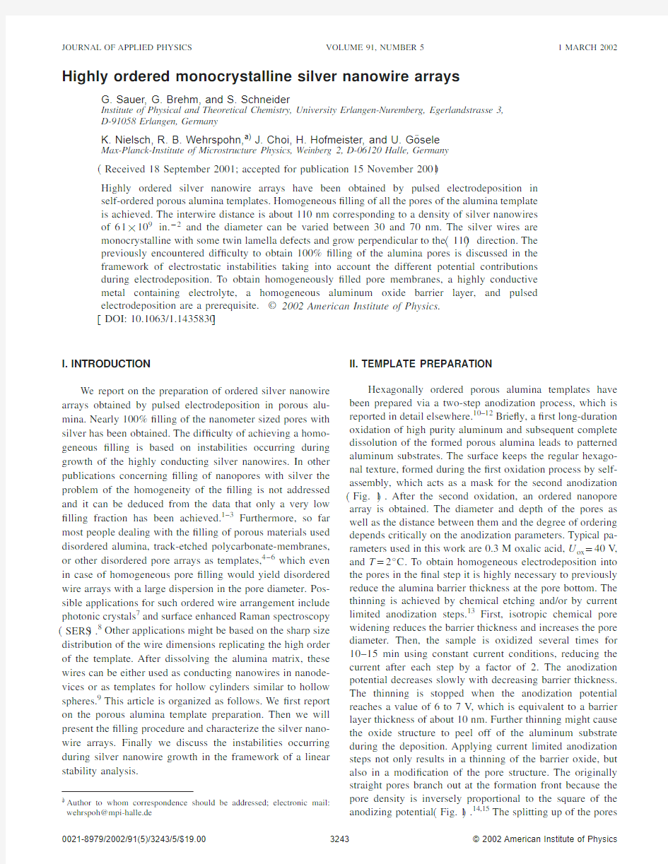
G. Sauer, G. Brehm, S. Schneider, K. Nielsch, R. B. Wehrspohn et al.
Citation: J. Appl. Phys. 91, 3243 (2002); doi: 10.1063/1.1435830
View online: https://www.sodocs.net/doc/5d949077.html,/10.1063/1.1435830
View Table of Contents: https://www.sodocs.net/doc/5d949077.html,/resource/1/JAPIAU/v91/i5
Published by the American Institute of Physics.
Related Articles
Highly ordered self-assembled nanoscale periodic faceting in GaAs(631) homoepitaxial growth
Appl. Phys. Lett. 101, 073112 (2012)
Diameter dependent optical emission properties of InAs nanowires grown on Si
Appl. Phys. Lett. 101, 053103 (2012)
Hole spectra and conductance for quantum wire systems under Rashba spin-orbit interaction
J. Appl. Phys. 110, 113705 (2011)
Structural and optical properties of m-plane GaN/AlGaN quantum wires grown by metalorganic chemical vapor deposition
Appl. Phys. Lett. 99, 113106 (2011)
Vibronic coupling in quantum wires: Applications to polydiacetylene
J. Chem. Phys. 135, 054906 (2011)
Additional information on J. Appl. Phys.
Journal Homepage: https://www.sodocs.net/doc/5d949077.html,/
Journal Information: https://www.sodocs.net/doc/5d949077.html,/about/about_the_journal
Top downloads: https://www.sodocs.net/doc/5d949077.html,/features/most_downloaded
Information for Authors: https://www.sodocs.net/doc/5d949077.html,/authors
Highly ordered monocrystalline silver nanowire arrays
G.Sauer,G.Brehm,and S.Schneider
Institute of Physical and Theoretical Chemistry,University Erlangen-Nuremberg,Egerlandstrasse3,
D-91058Erlangen,Germany
K.Nielsch,R.B.Wehrspohn,a)J.Choi,H.Hofmeister,and U.Go¨sele
Max-Planck-Institute of Microstructure Physics,Weinberg2,D-06120Halle,Germany
?Received18September2001;accepted for publication15November2001?
Highly ordered silver nanowire arrays have been obtained by pulsed electrodeposition in self-ordered porous alumina templates.Homogeneous?lling of all the pores of the alumina template is achieved.The interwire distance is about110nm corresponding to a density of silver nanowires of61?109in.?2and the diameter can be varied between30and70nm.The silver wires are monocrystalline with some twin lamella defects and grow perpendicular to the?110?direction.The previously encountered dif?culty to obtain100%?lling of the alumina pores is discussed in the framework of electrostatic instabilities taking into account the different potential contributions during electrodeposition.To obtain homogeneously?lled pore membranes,a highly conductive metal containing electrolyte,a homogeneous aluminum oxide barrier layer,and pulsed electrodeposition are a prerequisite.?2002American Institute of Physics.
?DOI:10.1063/1.1435830?
I.INTRODUCTION
We report on the preparation of ordered silver nanowire arrays obtained by pulsed electrodeposition in porous alu-mina.Nearly100%?lling of the nanometer sized pores with silver has been obtained.The dif?culty of achieving a homo-geneous?lling is based on instabilities occurring during growth of the highly conducting silver nanowires.In other publications concerning?lling of nanopores with silver the problem of the homogeneity of the?lling is not addressed and it can be deduced from the data that only a very low ?lling fraction has been achieved.1–3Furthermore,so far most people dealing with the?lling of porous materials used disordered alumina,track-etched polycarbonate-membranes, or other disordered pore arrays as templates,4–6which even in case of homogeneous pore?lling would yield disordered wire arrays with a large dispersion in the pore diameter.Pos-sible applications for such ordered wire arrangement include photonic crystals7and surface enhanced Raman spectroscopy ?SERS?.8Other applications might be based on the sharp size distribution of the wire dimensions replicating the high order of the template.After dissolving the alumina matrix,these wires can be either used as conducting nanowires in nanode-vices or as templates for hollow cylinders similar to hollow spheres.9This article is organized as follows.We?rst report on the porous alumina template preparation.Then we will present the?lling procedure and characterize the silver nano-wire arrays.Finally we discuss the instabilities occurring during silver nanowire growth in the framework of a linear stability analysis.II.TEMPLATE PREPARATION
Hexagonally ordered porous alumina templates have
been prepared via a two-step anodization process,which is
reported in detail elsewhere.10–12Brie?y,a?rst long-duration
oxidation of high purity aluminum and subsequent complete
dissolution of the formed porous alumina leads to patterned
aluminum substrates.The surface keeps the regular hexago-
nal texture,formed during the?rst oxidation process by self-
assembly,which acts as a mask for the second anodization ?Fig.1?.After the second oxidation,an ordered nanopore array is obtained.The diameter and depth of the pores as
well as the distance between them and the degree of ordering
depends critically on the anodization parameters.Typical pa-
rameters used in this work are0.3M oxalic acid,U ox?40V, and T?2°C.To obtain homogeneous electrodeposition into
the pores in the?nal step it is highly necessary to previously
reduce the alumina barrier thickness at the pore bottom.The
thinning is achieved by chemical etching and/or by current
limited anodization steps.13First,isotropic chemical pore
widening reduces the barrier thickness and increases the pore
diameter.Then,the sample is oxidized several times for
10–15min using constant current conditions,reducing the
current after each step by a factor of2.The anodization
potential decreases slowly with decreasing barrier thickness.
The thinning is stopped when the anodization potential
reaches a value of6to7V,which is equivalent to a barrier
layer thickness of about10nm.Further thinning might cause
the oxide structure to peel off of the aluminum substrate
during the deposition.Applying current limited anodization
steps not only results in a thinning of the barrier oxide,but
also in a modi?cation of the pore structure.The originally
straight pores branch out at the formation front because the
pore density is inversely proportional to the square of the
anodizing potential?Fig.1?.14,15The splitting up of the pores
a?Author to whom correspondence should be addressed;electronic mail:
wehrspoh@mpi-halle.de
JOURNAL OF APPLIED PHYSICS VOLUME91,NUMBER51MARCH2002
3243
0021-8979/2002/91(5)/3243/5/$19.00?2002American Institute of Physics
into the barrier layer leads to the formation of several nucle-ation sites in each pore at the beginning of the electrodepo-sition.Since the potential drop at the deposition interface depends critically on the barrier thickness,it has to be highly uniform.This is achieved by our thinning process described above.
III.ELECTRODEPOSITION
The pores are ?lled with silver under constant current conditions adopting the concept of pulsed electrodeposition.To achieve homogeneous ?lling of the pores,the choice of a suitable electrolyte is crucial.In order to avoid corrosive attack of the alumina template,the p H of the electrolyte has to be adjusted between 4and 8.16Therefore it is hardly pos-sible to work with cyanide containing silver baths,which generally require a higher p H.To supply the deposition in-terface suf?ciently fast with metal ions the concentration of electroactive silver species has to be as high as possible,otherwise hydrogen evolution can become dominant.Fur-thermore,pulsed electrodeposition through an insulating bar-rier layer requires high negative polarization (U pulse as high as ?8V ?.Consequently,the electrolyte must not contain other electroactive species like,e.g.,nitrate ions,which also might react in side reactions under these conditions.Finally,stability analysis shows ?see below ?that the conductivity in the electrolyte has to be quite high to obtain uniform depo-sition into the pores.Based on these considerations the choice of a suitable electrolyte is not trivial.As the presence of nitrate ions and other electroactive species is excluded silver sulfate ?8.5g/l ?was chosen as the silver ion source.Diammoniumhydrogencitrate ?200g/l ?was added to ensure a high conductivity and to adjust the p H value to around 4.5.Furthermore,diammoniumhydrogencitrate has the function of a repairing agent as it favors the formation of stable alu-mina during the positive polarization in the pulse sequence
?see below ?.Finally,the electrolyte contained potassiumthio-cyanate ?105g/l ?,which was necessary to dissolve precipi-tated silver salt through complexation.The pulsed elec-trodeposition consists of modulated pulses in the millisecond range ?Fig.2?.During each pulse of negative current (t pulse ?6ms,I pulse ?15mA/cm 2),silver is deposited at the pore bottom.A relatively high current density is applied in order to increase the number of nucleation sites in each pore.12After the deposition pulse,another pulse with positive polar-ization (t pulse ?6ms,U pulse ?6V ?was applied to discharge the capacitance of the barrier layer and to interrupt the elec-tric ?eld at the deposition interface immediately.The posi-tive pulse also repairs discontinuities in the barrier oxide,an important mechanism especially at the beginning of the elec-trodeposition.The current for this second pulse is also lim-ited to I max ?15mA/cm 2.To avoid depletion of the silver ions at the deposition interface,the ion concentration has to recover before the next double pulse is applied.Introducing a delay time t off of typically 0.4–1s is suf?cient to ensure the restoration of a high silver concentration at the pore bottom before the subsequent deposition pulse appears.This im-proves the homogeneity of the deposition and prevents ex-cessive hydrogen evolution.During the electrodeposition,the potential required to ensure the desired current density is measured for each pulse.Hence the electrodeposition can easily be followed via a potential versus pulse number plot ?Fig.3?.Generally,the plot can be divided into three regions.At the beginning of the ?lling process the electrons have to tunnel through the barrier oxide before they react with the silver ions and nucleation takes place at numerous sites in each pore.The surface available for electrodeposition is quite large.Further electrodeposition leads to a ?lling of the branched structure and thus the electrochemically active sur-face area decreases,accompanied by an increase in the depo-sition potential ??rst region ?.When the deposited
silver
FIG.1.Schematic diagram describing the fabrication of a highly ordered porous alumina matrix and the preparative steps necessary for the subse-quent ?lling of the structure.The Al substrate is prestructured by a long-time anodizing until the pores arrange in a hexagonal lattice.Then the aluminum oxide is selectively removed.Starting from a prestructured Al substrate,a highly ordered alumina pore structure is obtained in a second anodization step.Afterwards,the barrier layer is thinned and the pores are widened by isotropic chemical etching.For further thinning of the barrier layer two current-limited anodization steps are used and dendrite pore formation oc-curred at the barrier layer.Then,the pores are ?lled by pulsed electrodepo-sition with
silver.
FIG.2.Current and potential transients during electrodeposition.First a current-limited negative pulse t pulse is applied to deposit Ag.Then a positive pulse is applied to discharge the capacitance of the alumina barrier layer.The cycle is repeated after t off in order to avoid depletion of metal ions near the deposition interface.
reaches the beginning of the straight part of the pores the increase in the deposition potential slows down distinctly,but still proceeds ?second region ?.The decreasing silver con-centration in the pore channel can be made responsible for a gentle increase in the deposition potential in this region,but it cannot explain the signi?cant rise of more than one volt.The ?lling of the pores continues until the deposition poten-tial drops or exhibits some noise ?third region ?,which is due to an increase of the electroactive surface arising from silver deposition on top of the porous alumina matrix.Although the signi?cant increase in the deposition potential,especially in the second region,is not completely understood yet,the po-tential versus pulse number plot at least allows one to follow and control the ?lling process.Additionally the charge can be calculated from the measured data and thus allows one to estimate the degree of pore ?lling and to control the wire length.
IV.CHARACTERIZATION
The ?lled alumina templates were examined by scanning electron microscopy ?SEM ?to determine the degree of pore ?lling and the extension of the silver nanowires.By etching the ?lled porous structure from the top,nanowires ending somewhat below the membrane surface became observable for scanning electron microscopy ?SEM ?examination.Etch-ing of the samples was performed by Ar sputtering with an ion mill ?Gatan Duo Mill 600?and led to a funnel-shaped excavation in the surface.The depth of the hole was corre-lated with the etching time.Figure 4shows two top view micrographs and one side view micrograph of a highly or-dered alumina pore structure ?lled with silver.The pore di-ameter is approximately 35nm and the interpore distance is 110nm.The thickness of the porous layer is approximately 2?m.Figure 4?a ?was taken before etching the sample.In some pores,the silver nanowires reached the pore opening and excessive electrodeposition yielded three-dimensional growth of silver particles on top of the matrix structure ?bright spots ?.In most of the remaining ?not completely ?lled ?pores,the top of the nanowires can be seen ?different gray levels indicate different levels of residual pore depth ?.Figure 4?b ?shows the same sample after etching the initially 2?m thick porous structure by about 200nm.As can be seen clearly,almost every pore is ?lled with silver to this level indicating ?uctuations in the height of the ?lling of less than 10%.The same information can be obtained from Fig.4?c ?.Simple cutting of an ?unthinned ?substrate with wire cutting pliers leads to a fracture of the rigid alumina layer.Most of the pores are ?lled with silver wires ?bright sticks ?to at least 90%in height.The lack of wires in some of the pores as well as the presence of twisted and ruptured wires can easily be explained by the mechanical stress evolving during the process of the cleavage of the alumina membrane.
Crystallinity and surface con?guration of the silver wires were further analyzed by high-resolution transmission elec-tron microscopy ?HRTEM ?.After dissolving the alumina ma-trix such wires have been placed on electron microscopy copper grids covered by a thin carbon ?lm.Although ar-ranged randomly on the carbon ?lm,the silver wires tend
to
FIG.3.V oltage-pulse-number curve during the ?lling process of porous alumina with Ag.In regime I the dendride-like nucleation pores are ?lled with Ag.The potential increases due to a reduction of the deposition area.In regime II the silver wires grow and the potential increases slightly.In regime III the silver wires reach the top of the alumina template and the noise and slight potential drop are due to the uncontrolled increase in deposition
area.
FIG.4.SEM micrographs of a silver-?lled alumina membrane.?a ?Top view of an unthinned sample,?b ?top view of the same sample approximately 200nm underneath the initial surface,and ?c ?side view of a fracture.
align parallel in groups because of capillary forces acting during evaporation of the solvent.Figure 5shows a HRTEM image of a segment of two adjacent wires touching each other along a nearly horizontal line.From selected area elec-tron diffraction these silver wires are found to be single crys-talline.Nevertheless,they contain a certain extent of lattice defects such as twin boundaries and stacking faults.While the wire in the lower part of Fig.5does not exhibit lattice defects in the frame of this image,the upper wire has three planar defects that may be recognized as narrow bands of stronger contrast running obliquely across the wire.Their structures are shown in more detail in the boxes beneath.From the course of the lattice plane fringes seen here,and re?ected also by the diffractogram ?Fourier transform ?of the image given in the circular inset,the ?110?zone axis of the silver lattice is deduced to be perpendicular to the wire axis.The wires have generally a face-centered-cubic ?fcc ?lattice,which was also con?rmed by x-ray diffraction analysis.They do not show indications of neither oxide coverage nor incor-poration.
V.DISCUSSION
As mentioned in the Introduction,most studies have not discussed the achieved degree of ?lling of the pores with either silver 1–3or other metals like Au,17Co,18–21Fe,22or Ni.23In the present work we demonstrated that under very speci?c conditions of pulsed electrodeposition,one can ob-tain a nearly 100%homogeneous ?lling of pore arrays also with silver.In a former publication we have shown that it is indeed possible to ?ll homogeneous nickel and cobalt into porous alumina.13
Now we are presenting a model to explain the physical reasons underlying this process.The key ingredients of our model are a thin homogeneous barrier layer,pulsed elec-trodeposition,and a highly conducting electrolyte.Figure 6shows a schematic diagram of the equivalent electrical cir-cuit applicable during pulsed electrodeposition.Starting from the current source,there is a resistance in the aluminum sub-strate (R s ),then all the pores are in parallel consisting of a thin interfacial oxide layer (R i ),the deposited metal (?m ),and the electrolyte (?e ).Finally,there is a common resis-tance of the electrolyte in the electrochemical cell (R e ).For a stability analysis,we can neglect the potential drop in the aluminum substrate and the electrolyte since they are simple series resistances and do not contribute signi?cantly to the instability.The ?rst instability arises from the fact that the alumina barrier layer at the pore bottom is not uniform.If it would be uniform,then it would represent an overall series resistance like R e or R s .However,due to the electrochemi-cal process,there are always ?uctuations in the barrier layer thickness.Therefore as already pointed out by Zagiel et al.,24the barrier layer thickness and therefore the overall potential drop iR i should be as small as possible compared to the potential drop across ?e and ?m .This is the reason for thin-ning the alumina barrier layer to typically 10nm.However,this still results in a signi?cant contribution to the potential drop of ?6V in the barrier layer compared to a few tenths mV for the electrolyte solution ?Table I ?.Therefore and be-cause of the rectifying nature of the barrier layer,we have applied a self-limiting current process by using pulsed elec-trodeposition.During the 6ms negative pulses,all of the metal ions in the pore are deposited due to the high current.Thus once all the ions have been deposited in one speci?c pore,the current ?ow is reduced and other pores with a slightly thicker barrier layer take over the current.A uniform ?lling of the pore bottom is achieved and the impact of ?uc-tuations of R i is reduced due to a time dependent electrolyte resistivity ?e ?t ?.During the positive pulse,the capacitance
of
FIG.5.HRTEM image of a segment of two adjacent silver nanowires.The upper one exhibits three planar defects shown in more detail in the box below.The diffractogram ?circular inset ?re?ects the lattice relation between the twin lamella ‘‘T’’and wire
matrix.
FIG.6.Schematic diagram of the electric circuit during pulsed electrodepo-sition.
TABLE I.Resistivities ?at 38°C ?of some metals and electrolytes used in this work and similar work in literature.
Material
Resistivity in ?cm
nickel ?bulk ? 6.3?10?6silver ?bulk ?
1.4?10?6
nickel Watts-bath electrolyte 14Metzger Co bath 77Xu Ni bath
500silver containing electrolyte ?this work ?
5.2
the barrier layer is discharged.Moreover,as pointed out by Dobrev et al.,25the use of positive pulses leads to monocrys-talline nanowires.They speculate that during the positive pulse,a certain amount of current will lead to the preferential dissolution of the defect rich metal deposit of the previous negative pulse,thus promoting monocrystalline growth.
Another electrostatic instability arises during the growth of the silver wires.Since the Ag nanowires are always more conductive than the electrolyte,small?uctuations in the length of the wire will be enhanced and will lead to nonuni-form growth.Similar to the case of pore growth in highly resistive p-type silicon,this effect can be described by a linear stability model.Following Wehrspohn et al.,26,27we can de?ne a instability coef?cient?
??
?e??m
?e?qR i??m q,?1?
where q is the?uctuation wavenumber?in cm?1).If?is negative,the metal wire front grows uniformly,i.e.,the?ll-
ing is homogeneous.If?is positive,the metal wire front will in general be unstable and an inhomogeneous?lling will
occur.The inverse1/?represents the typical length for which one silver wire will start to grow faster in one pore
than in the others.To obtain a homogeneous?lling because
of negative?,the resistivity of the electrolyte must be lower than that of the metal wire.Such a condition is unrealistic for
any metal since the conductivity of pure metals????cm?is a few orders of magnitude higher than that of concentrated
electrolytes(?10?cm?.The only possibility to?ll a thin
layer of porous alumina rather homogeneously is therefore to
increase1/?so that it is larger than the membrane thickness. This means the onset of the instability will not occur below
this critical thickness and a homogeneous?lling is possible.
Since?m??e,the critical thickness1/?simpli?es to1/??1/q?R i/?e.For q?105cm?1,R i?36?cm2for a cur-rent density I?15mA/cm2and a porosity of9%,?e?10?cm,1/?is limited by the term R i/?e,i.e.,interface or barrier-layer limited.Thus the barrier layer thickness is pro-
portional to the critical thickness1/?and the conductivity of the electrolyte is inversely proportional to1/?.This under-lines the importance of using highly conductive electrolytes like Watts-bath-type electrolytes in the case of Ni and Co nanowires.Indeed,the Xu group28and the Metzger group29 both obtain very good Ni?lling degrees in alumina pore arrays applying these rules.Xu uses barrier layer thinning, pulsed electrodeposition,and high temperature deposition to increase the mobility of the ions in the organic electrolyte.28 Metzger uses pulsed electrodeposition,barrier layer thinning, and also highly conducting electrolytes.However,in both studies,the resistivities are much higher than for the Watts-bath type electrolyte used in our work.13Therefore instabili-ties have to be compensated in these groups by decreased pulse duration.However,a drawback of the latter strategy is that a thicker barrier layer has to be used to reduce the dis-charge time of the barrier layer capacitance.The thicker bar-rier layer leads to signi?cantly higher overpotentials during deposition and to a worse crystallinity of the nanowires.29VI.CONCLUSIONS
A highly ef?cient method of depositing silver into the nanochannels of ordered porous alumina is presented.Nearly 100%of the pores were?lled with silver and only small ?uctuations in the growth rate in different pores were ob-served.The silver nanowires are monocrystalline with some twin-lamella defects.The growth direction is perpendicular to the?110?direction.The wire diameter can be varied from 30to70nm depending on how the alumina template is pre-pared.Based on a linear stability analysis,we have modeled the electrochemical?lling behavior.To obtain homoge-neously?lled pore membranes,a homogeneous aluminum oxide barrier layer,pulsed electrodeposition,and a highly conductive electrolyte are a prerequisite. ACKNOWLEDGMENTS
The authors thank S.Hopfe for the SEM sample prepa-rations and Dr.H.-N.Lee for the x-ray measurements.
1Q.Zhang,Y.Li,D.Xu,and Z.Gu,J.Mater.Sci.Lett.20,925?2001?. 2I.Mikuslkas et al.,Opt.Mater.17,343?2001?.
3F.Mu¨ller,A.D.Mu¨ller,M.Kro¨ll,and G.Schmid,Appl.Surf.Sci.171, 125?2001?.
4X.Jiang et al.,J.Mater.Chem.11,1775?2001?.
5V.M.Cepak and C.R.Martin,J.Phys.Chem.B102,9985?1998?.
6N.F.Jana et al.,https://www.sodocs.net/doc/5d949077.html,mun.?Cambridge?7,617?2001?.
7H.van der Lem and A.Moroz,J.Opt.2,395?2000?.
8G.Sauer?unpublished?.
9F.Caruso,R.A.Caruso,and H.Mo¨hwald,Chem.Mater.11,3309?1999?. 10H.Masuda and K.Fukuda,Science268,1466?1995?.
11H.Masuda,K.Yada,and A.Osaka,Jpn.J.Appl.Phys.,Part237,L1340?1998?.
12O.Jessensky,F.Mu¨ller,and U.Go¨sele,Appl.Phys.Lett.72,1173?1998?. 13K.Nielsch,F.Mu¨ller,A.-P.Li,and U.Go¨sele,Adv.Mater.12,582?2000?. 14F.Keller,M.S.Hunter,and D.L.Robinson,J.Electrochem.Soc.100,411?1953?.
15A.-P.Li,F.Mu¨ller,A.Birner,K.Nielsch,and U.Go¨sele,J.Appl.Phys. 84,6023?1998?.
16P.P.Mardilovich,https://www.sodocs.net/doc/5d949077.html,yadinov,N.I.Mazurenko,and R.Paterson,J. Membr.Sci.98,143?1995?.
17X.Y.Zhang et al.,J.Mater.Chem.11,1732?2001?.
18H.Zeng,M.Zheng,R.Skomski,D.J.Sellmyer,Y.Liu,L.Menon,and S. Bandyopadhyay,J.Appl.Phys.87,4718?2000?.
19A.Kazadi Mukenga Bantu et al.,J.Appl.Phys.89,3393?2001?.
20T.Thurn-Albrecht,J.Schotter,G.A.Ka¨stle,N.Emley,T.Shibauchi,L. Krusin-Elbaum,K.Guarini,C.T.Black,M.T.Tuominen,and T.P.Rus-sell,Science290,2126?2000?.
21H.Q.Cao,Z.Xu,H.Sang,D.Sheng,and C.Y.Tie,Adv.Mater.13,121?2001?.
22Y.Peng,H.-L.Zhang,S.-L.Pan,and H.-L.Li,J.Appl.Phys.87,7405?2000?.
23P.M.Paulus,F.Luis,M.Kro¨ll,G.Schmid,and L.J.de Jongh,J.Magn. Magn.Mater.224,180?2001?.
24A.Zagiel,P.Natishan,and E.Gileadi,Electrochim.Acta35,1019?1990?. 25D.Dobrev,J.Vetter,N.Angert,and R.Neumann,Appl.Phys.A:Mater. Sci.Process.69,233?1999?.
26R.B.Wehrspohn,J.-N.Chazalviel,and F.Ozanam,J.Electrochem.Soc. 145,2958?1998?.
27R.B.Wehrspohn,F.Ozanam,and J.-N.Chazalviel,J.Electrochem.Soc. 146,3309?1999?.
28A.J.Yin,J.Li,W.Jian,A.J.Bennett,and J.M.Xu,Appl.Phys.Lett.79, 1039?2001?.
29M.Sun,G.Zangari,M.Shamsuzzoha,and R.M.Metzger,Appl.Phys. Lett.78,2964?2001?.