msg2133_ds_v01

FEATURES
n Capacitive Touch Screen Controller
?Supports up to 30 sensors
?Supports screen size up to 5”
?X, Y resolution up to 2048 pixels x 2048 pixels ?Programmable reporting rate: max 5ms/report ?Accurate single-touch coordinate report and two-touch gesture
?Automatic background capacitance tracking
?14-bit ADC n Hardware
?32-bit MCU
?SRAM embedded
?I2C slave interface, up to 400Kb/s ?Built-in oscillator
n Operation Voltage
? 2.8V ~ 3.3V
n Misc.
?QFN-40 package
GENERAL DESCRIPTION
The MSG2133 is a capacitive touch screen controller. The internal ADC & DSP circuitry implement high-accuracy self-capacitance measurement. A 32-bit MCU with embedded SRAM provides programmability to suffice different requirements of various touch screen designs.
BLOCK DIAGRAM
Doc. No.: 2011080084
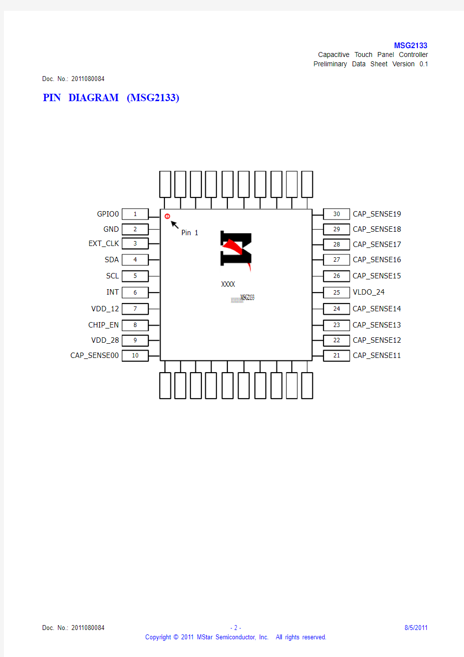
PIN DIAGRAM (MSG2133)
C A P _S E N S E 01
C A P _S E N S E 02
15
16
C A P _S E N S E 21
C A P _S E N S E 20
VDD_12EXT_CLK
GPIO0CAP_SENSE00
SCL SDA INT CHIP_EN VDD_28GND C A P _S E N S E 06
C A P _S E N S E 05
C A P _S E N S E 09
C A P _S E N S E 08
C A P _S E N S E 07
C A P _S E N S E 03
C A P _S E N S E 04
C A P _S E N S E 10
CAP_SENSE14CAP_SENSE13CAP_SENSE12CAP_SENSE11
CAP_SENSE19CAP_SENSE18CAP_SENSE17CAP_SENSE16CAP_SENSE15VLDO_24C A P _S E N S E 24
C A P _S E N S E 23
C A P _S E N S E 22
C A P _S E N S E 25
C A P _S E N S E 26
C A P _S E N S E 27
C A P _S E N S E 28
C A P _S E N S E 29
MSG2133
XXXXXXXXXXX XXXX X
Doc. No.: 2011080084
Doc. No.: 2011080084
PIN DESCRIPTION
Capacitive Touch Sensor Interface
Pin Name Pin Type Function Pin CAP_SENSE00 Analog Input Capacitive touch sensor input 10 CAP_SENSE01 Analog Input Capacitive touch sensor input 11 CAP_SENSE02 Analog Input Capacitive touch sensor input 12 CAP_SENSE03 Analog Input Capacitive touch sensor input 13 CAP_SENSE04 Analog Input Capacitive touch sensor input 14 CAP_SENSE05 Analog Input Capacitive touch sensor input 15 CAP_SENSE06 Analog Input Capacitive touch sensor input 16 CAP_SENSE07 Analog Input Capacitive touch sensor input 17 CAP_SENSE08 Analog Input Capacitive touch sensor input 18 CAP_SENSE09 Analog Input Capacitive touch sensor input 19 CAP_SENSE10 Analog Input Capacitive touch sensor input 20 CAP_SENSE11 Analog Input Capacitive touch sensor input 21 CAP_SENSE12 Analog Input Capacitive touch sensor input 22 CAP_SENSE13 Analog Input Capacitive touch sensor input 23 CAP_SENSE14 Analog Input Capacitive touch sensor input 24 CAP_SENSE15 Analog Input Capacitive touch sensor input 26 CAP_SENSE16 Analog Input Capacitive touch sensor input 27 CAP_SENSE17 Analog Input Capacitive touch sensor input 28 CAP_SENSE18 Analog Input Capacitive touch sensor input 29 CAP_SENSE19 Analog Input Capacitive touch sensor input 30 CAP_SENSE20 Analog Input Capacitive touch sensor input 31 CAP_SENSE21 Analog Input Capacitive touch sensor input 32 CAP_SENSE22 Analog Input Capacitive touch sensor input 33 CAP_SENSE23 Analog Input Capacitive touch sensor input 34 CAP_SENSE24 Analog Input Capacitive touch sensor input 35 CAP_SENSE25 Analog Input Capacitive touch sensor input 36 CAP_SENSE26 Analog Input Capacitive touch sensor input 37 CAP_SENSE27 Analog Input Capacitive touch sensor input 38 CAP_SENSE28 Analog Input Capacitive touch sensor input 39 CAP_SENSE29 Analog Input Capacitive touch sensor input 40
Doc. No.: 2011080084
Host Interface
Pin Name Pin Type Function Pin CHIP_EN Input w/ 5V-tolerant Chip Enable 8 EXT_CLK Input w/ 5V-tolerant External Sync Clock Input 3 SDA I/O w/ 5V-tolerant I2C Serial Data Input/Output 4 SCL I/O w/ 5V-tolerant I2C Serial Clock Input/Output 5 INT I/O w/ 5V-tolerant Interrupt signal; active low 6
GPIO Interface
Pin Name Pin Type Function Pin GPIO0 I/O w/ 5V-tolerant General Purpose Input/Output; 4mA driving strength 1
Power Pins
Pin Name Pin Type Function Pin VDD_28 2.8V Power 2.8V~3.3V power supply; connect 1uF capacitor to Ground 9
25 VLDO_24 2.4V Power Internally generated reference voltage; connect 1uF
capacitor to Ground
7 VDD_12 1.2V Power Internally generated digital power supply; connect 1uF
capacitor to Ground
GND Ground Ground Note 2 Note: E-pad should be connected to system GND net.
Doc. No.: 2011080084
ELECTRICAL SPECIFICATIONS
Parameter Min Typ Max Unit DIGITAL INPUTS
Input Voltage 1, High (V IH1)1 1 V Input Voltage 2, High (V IH2)2 2 V Input Voltage, Low (V IL) 0.3 V DIGITAL OUTPUTS
Output Voltage, High (V OH) V VDD - 0.1 V Output Voltage, Low (V OL) 0.1 V Specifications are subjected to change without notice.
Notes:
1.V IH1 includes pins EXT_CLK, SDA, SCL, INT, GPIO0.
2.V IH2 refers to other digital pins.
Recommended Operating Power Conditions
Parameter Symbol Min Typ Max Unit Power Supply V VDD 2.8 - 3.3 V
Absolute Maximum Ratings
stress rating only and does not imply functional operation of the device. Exposure to absolute maximum ratings for extended periods may affect device reliability.
ORDERING GUIDE
Part Number
Temperature Range
Package Description
Package Option MSG2133
-10°C to +85°C QFN
40
MARKING INFORMATION
MSG2133
Operation Code B Date Code (YYWW)
Lot Number
Operation Code A Part Number
DISCLAIMER
MSTAR SEMICONDUCTOR RESERVES THE RIGHT TO MAKE CHANGES WITHOUT FURTHER NOTICE TO ANY PRODUCTS HEREIN TO IMPROVE RELIABILITY, FUNCTION OR DESIGN. NO RESPONSIBILITY IS ASSUMED BY MSTAR SEMICONDUCTOR ARISING OUT OF THE APPLICATION OR USER OF ANY PRODUCT OR CIRCUIT DESCRIBED HEREIN; NEITHER DOES IT CONVEY ANY LICENSE UNDER ITS PATENT RIGHTS, NOR THE RIGHTS OF OTHERS.
REVISION HISTORY
Document Description Date MSG2133_ds_v01 ? Initial release
Aug 2011
Electrostatic charges accumulate on both test equipment and human body and can discharge without detection. MSG2133 comes with ESD protection circuitry; however, the device may be permanently damaged when subjected to high energy discharges. The device should be handled with proper ESD precautions to prevent malfunction and performance degradation.
Doc. No.: 2011080084
MECHANICAL DIMENSIONS
holes below MStar IC. There should only be ground plane in this area. E-pad should be connected to system GND net.
Doc. No.: 2011080084
REGISTER DESCRIPTION ISP Register (Bank = 08)
ISP Register (Bank = 08)
Index (Absolute) Mnemonic Bit Description REG0800
7:0 Default : 0x55
Access : R/W
00h
(0800h)
ISP_PASSWORD[7:0]
7:0
ISP Password 0xAAAA,
If password is correct, enable ISP. If password is incorrect, disable ISP. REG0801
7:0 Default : 0x55
Access : R/W
00h
(0801h) ISP_PASSWORD[15:8] 7:0 See description of '0800h'. REG0802
7:0 Default : 0x00
Access : WO 01h
(0802h)
SPI_COMMAND[7:0] 7:0 SPI command,
If write data to this port, ISP will start operation. REG0804 7:0 Default : 0x00 Access : R/W
02h
(0804h) ADDRESS1[7:0] 7:0 SPI address 1, A[7:0]. REG0805 7:0 Default : 0x00 Access : R/W 02h
(0805h) ADDERSS2[7:0] 7:0 SPI address 2, A[15:8]. REG0806 7:0 Default : 0x00 Access : R/W 03h
(0806h) ADDRESS3[7:0] 7:0 SPI address 3, A[23:16]. REG0808 7:0 Default : 0x00 Access : WO 04h
(0808h) WDATA[7:0] 7:0 SPI write data register. REG080A 7:0 Default : 0x00 Access : RO 05h
(080Ah) RDATA[7:0] 7:0 SPI read data register. REG080C 7:0 Default : 0x04
Access : R/W SPI_CLK_DIV16 7 SPI_CLOCK = MCU_CLOCK/16. SPI_CLK_DIV8 6 SPI_CLOCK = MCU_CLOCK/8. SPI_CLK_DIV7 5 Reserved. SPI_CLK_DIV6 4 Reserved. SPI_CLK_DIV5 3 Reserved.
SPI_CLK_DIV4 2 SPI_CLOCK = MCU_CLOCK/4. SPI_CLK_DIV3 1 Reserved.
06h
(080Ch)
SPI_CLK_DIV2
0 SPI_CLOCK = MCU_CLOCK/2. REG080D 7:0 Default : 0x00 Access : R/W
-
7:3 Reserved.
06h
(080Dh)
SPI_CLK_DIV128
2
SPI_CLOCK = MCU_CLOCK/128.
Doc. No.: 2011080084
ISP Register (Bank = 08)
Index (Absolute)
Mnemonic
Bit
Description
SPI_CLK_DIV64 1 SPI_CLOCK = MCU_CLOCK/64. SPI_CLK_DIV32
0 SPI_CLOCK = MCU_CLOCK/32. REG080E 7:0 Default : 0x00 Access : R/W
-
7:3 Reserved. 07h
(080Eh)
DEVICE_SELECT[2:0]
2:0
Select Device. 000: PMC.MXIC. 001: NextFlash. 010: ST. 011: SST. 100: ATMEL. REG0810 7:0 Default : 0x00 Access : WO -
7:1 Reserved.
08h
(0810h)
SPI_CE_CLR
SPI chip enable clear.
Software can force SPI chip disable at burst SPI read/write, this bit is write-then-clear register. 1: For clear. 0: For not clear. REG0812 7:0 Default : 0x01
Access : R/W 09h
(0812h)
TCES_TIME[7:0]
7:0
SPI Chip enable setup/hold time. 0x0000: Delay 1 SPI clock. 0x0001: Delay 2 SPI clock. 0x000f: Delay 16 SPI clock. 0xffff: Delay 64k SPI clock. Default delay 2 SPI clock. REG0813 7:0 Default : 0x00
Access : R/W
09h
(0813h) TCES_TIME[15:8] 7:0 See description of '0812h'. REG0814 7:0 Default : 0xF3
Access : R/W 0Ah
(0814h)
TBP_TIME[7:0]
7:0
Byte-Program time for device SST. 0x0000: Delay 1 SPI clock. 0x0001: Delay 2 SPI clock. 0x000f: Delay 16 SPI clock. 0xffff: Delay 64k SPI clock. Default delay 500 SPI clock,
Assume SPI clock 40ns, Delay 500*40 = 20 us. REG0815 7:0 Default : 0x01
Access : R/W
0Ah
(0815h)
TBP_TIME[15:8]
7:0
See description of '0814h'.
Doc. No.: 2011080084
ISP Register (Bank = 08)
Index (Absolute) Mnemonic
Bit
Description
REG0816 7:0 Default : 0x04
Access : R/W
0Bh
(0816h)
TCEH_TIME[7:0]
7:0
SPI Chip enable pulse high time. 0x0000: Delay 1 SPI clock. 0x0001: Delay 2 SPI clock. 0x000f: Delay 16 SPI clock. 0xffff: Delay 64k SPI clock. Default delay 5 SPI clock. REG0817 7:0 Default : 0x00
Access : R/W
0Bh
(0817h) TCEH_TIME[15:8] 7:0 See description of '0816h'. REG0818 7:0 Default : 0x00 Access : WO -
7:1 Reserved.
0Ch
(0818h)
SPI_RD_REQ
0 SPI READ Data Request, For CPU read SPI data via RIU, If CPU read SPI data via XIU, request not needed. REG081A 7:0 Default : 0x14
Access : R/W 0Dh
(081Ah) ISP_RP_ADR1[7:0] 7:0 Programmable ISP Read port address[15:0]. REG081B
7:0 Default : 0xC2
Access : R/W
0Dh
(081Bh) ISP_RP_ADR1[15:8] 7:0 See description of '081Ah'. REG081C 7:0 Default : 0x81
Access : R/W 0Eh
(081Ch) ISP_RP_ADR2[7:0] 7:0 Programmable ISP Read port address[31:0]. REG081D
7:0 Default : 0x1F
Access : R/W
0Eh
(081Dh) ISP_RP_ADR2[15:8] 7:0 See description of '081Ch'. REG081E 7:0 Default : 0x01 Access : R/W
-
7:1 Reserved.
0Fh
(081Eh)
ENDIAN_SEL_SPI
0 0: BIG_ENDIAN. 1: LITTLE_ENDIAN. REG0820 7:0 Default : 0x00 Access : RO
-
7:1 Reserved. 10h
(0820h)
ISP_ACTIVE
0 ISP ACTIVE FLAG. REG0822 7:0 Default : 0x00 Access : RO
-
7:2 Reserved.
CPU_ACTIVE 1 CPU_ACTIVE FLAG. 11h
(0822h)
-
0 Reserved. REG0824 7:0 Default : 0x00 Access : RO
12h
(0824h)
-
7:3
Reserved.
Doc. No.: 2011080084
ISP Register (Bank = 08)
Index (Absolute)
Mnemonic
Bit
Description
DMA_ACTIVE 2 DMA_ACTIVE FLAG. -
1:0 Reserved. REG082A 7:0 Default : 0x00 Access : RO
-
7:1 Reserved.
15h
(082Ah)
SPI_RD_DATA_RDY
SPI Read Data Ready flag. 1: Read data ready. 0: Read data not ready. REG082C 7:0 Default : 0x00 Access : RO -
7:1 Reserved.
16h
(082Ch)
SPI_WR_DATA_RDY
SPI Write Ready flag. 1: Write data ready. 0: Write data not ready. REG082E 7:0 Default : 0x00 Access : RO -
7:1 Reserved.
17h
(082Eh)
SPI_WR_CM_RDY
SPI Write Command Ready flag. 1: Write command ready. 0: Write command not ready. REG0830 7:0 Default : 0x00 Access : R/W -
7:1 Reserved.
18h
(0830h)
CPU_RST_FM_ISP
ISP generate reset to CUP,
When ISP programming done, software maybe can. Issue a reset to CPU. REG0832 7:0 Default : 0x00 Access : RO -
7:1 Reserved.
19h
(0832h)
ISP_OLD_EN
0 Read flag, for ISP_OLD_EN. REG0842 7:0 Default : 0x00
Access : R/W 21h
(0842h)
AAI_NUM[7:0]
7:0
For SST SPI FLASH USE.
At AAI mode, set how many data will be written. 0x0000: For 1 byte programming. 0x0001: For 2 byte programming. 0xFFFF: For 64k byte programming. REG0843 7:0 Default : 0x00
Access : R/W
21h
(0843h) AAI_NUM[15:8] 7:0 See description of '0842h'. 22h
REG0844
7:0
Default : 0x00
Access : R/W Doc. No.: 2011080084
ISP Register (Bank = 08)
Index (Absolute) Mnemonic
Bit
Description
PAGE_PRO_REG 7 FORCE SPI COMMAND.
Force PAGE PROGRAMMING. FAST_READ_REG 6 FORCE SPI COMMAND. Force FAST READ. READ_REG 5 FORCE SPI COMMAND. Force READ.
WRCR_REG 4 FORCE SPI COMMAND. Force WRCR.
RDCR_REG 3 FORCE SPI COMMAND. Force RDCR.
WRSR_REG 2 FORCE SPI COMMAND. Force WRSR.
RDSR_REG 1 FORCE SPI COMMAND. Force RDSR.
(0844h)
AAI_REG
0 FORCE SPI COMMAND. Force AAI mode. REG0845 7:0 Default : 0x00 Access : R/W
-
7:2 Reserved.
MAN_ID_REG 1 FORCE SPI COMMAND.
Force READ MANUFACTURER ID. 22h
(0845h)
B_ERASE_REG
0 FORCE SPI COMMAND. Force BLOCK ERASE. REG084A 7:0 Default : 0x00
Access : R/W 25h
(084Ah)
TEST_MODE[7:0]
7:0
TEST_MODE,
User define SPI waveform, 0x7777: User define. Others: Not User define,
Before entry TEST_MODE, Please make sure. ISP/DMA disable. REG084B 7:0 Default : 0x00
Access : R/W
25h
(084Bh) TEST_MODE[15:8] 7:0 See description of '084Ah'. REG084C 7:0 Default : 0x01 Access : R/W -
7:1 Reserved.
26h
(084Ch)
TEST_SPI_CEB 0 User generates SPI chip enable waveform. 27h
REG084E
7:0
Default : 0x00
Access : R/W Doc. No.: 2011080084
ISP Register (Bank = 08)
Index (Absolute) Mnemonic
Bit
Description
-
7:1 Reserved.
(084Eh)
TEST_SPI_SCK
0 User generates SPI clock waveform. REG0850 7:0 Default : 0x01 Access : R/W
-
7:1 Reserved.
28h
(0850h)
TEST_SPI_SI
0 User generates SPI data waveform. REG0852 7:0 Default : 0x00 Access : RO -
7:1 Reserved.
29h
(0852h)
TEST_SPI_SO
SPI Data output. For RIU read.
Please delay 1us for every setting (TEST MODE). EX1.
W(0x21,0x0) --> delay 1us --> W(0x23,0x1) -->. Delay 1us --> W(0x22,0x1) --> delay 1us -->.
W(0x22,0x0) --> delay 1us ........--> W(ox21,0x1). EX2.
W(0x21,0x0) --> delay 1us --> W(0x22,0x1) -->. Delay 1us --> W(0x22,0x0) --> delay 1us -->. R(0x24) --> delay 1us .........> W(0x21,01). REG0854
7:0 Default : 0x00
Access : R/W 2Ah
(0854h)
TRIGGER_MODE[7:0]
7:0
TRIGGER_MODE,,
0x3333: Trigger mode. others: Not Trigger mode.
Before entry Trigger mode, Please make sure. ISP/DMA disable. REG0855
7:0 Default : 0x00
Access : R/W
2Ah
(0855h) TRIGGER_MODE[15:8] 7:0 See description of '0854h'. REG085E 7:0 Default : 0x00 Access : R/W -
7:4 Reserved.
BRANCH_COUNTER_START
3
Start counter for CPU branch. 1: Start. 0: Not Start.
BRANCH_COUNTER_CLEAR 2
Clear counter for CPU branch. 1: Clear. 0: Not Clear. 2Fh
(085Eh)
-
1:0 Reserved. 30h
REG0860
7:0
Default : 0x00
Access : WO Doc. No.: 2011080084
ISP Register (Bank = 08)
Index (Absolute) Mnemonic Bit Description -
7:1 Reserved.
(0860h)
DMA_START
0 DMA Start, DMA between MIU and SPI device. REG0862 7:0 Default : 0x00
Access : R/W
31h
(0862h) DMA_CNT[7:0] 7:0 DMA Transfer size (byte), REG0863 7:0 Default : 0x00
Access : R/W 31h
(0863h) DMA_CNT[15:8] 7:0 See description of '0862h'. REG0864
7:0 Default : 0x00
Access : R/W 32h
(0864h)
DMA_MIU_START_ADR1[7:0] 7:0 DMA source address, Unit word address,
MIU_ADDRESS[15:0]. REG0865
7:0 Default : 0x00
Access : R/W
32h
(0865h) DMA_MIU_START_ADR1[15:8] 7:0 See description of '0864h'. REG0866
7:0 Default : 0x00
Access : R/W 33h
(0866h)
DMA_MIU_START_ADR2[7:0] 7:0 DMA source address, Unit word address, MIU_ADDRESS[31:16]. REG0867
7:0 Default : 0x00
Access : R/W
33h
(0867h) DMA_MIU_START_ADR2[15:8] 7:0 See description of '0866h'. REG0868 7:0 Default : 0x00 Access : RO
-
7:2 Reserved. DMA_DONE 1 DMA done FLAG. 34h
(0868h)
DMA_BUSY
0 DMA busy FLAG. REG086A
7:0 Default : 0x00 Access : RO
35h
(086Ah) DMA_CNT_STATUS[7:0] 7:0 DMA counter status. REG086B
7:0 Default : 0x00
Access : RO
35h
(086Bh) DMA_CNT_STATUS[15:8] 7:0 See description of '086Ah'. REG086C 7:0 Default : 0x01 Access : R/W
CHIP_SELECT8 7 Reserved, No use. CHIP_SELECT7 6 Reserved, No use. CHIP_SELECT6 5 Reserved, No use. CHIP_SELECT5 4 Reserved, No use. CHIP_SELECT4 3 Reserved, No use. CHIP_SELECT3 2 Reserved, No use. CHIP_SELECT2 1 Reserved, No use. 36h
(086Ch)
CHIP_SELECT1
Reserved, No use.
Doc. No.: 2011080084
ISP Register (Bank = 08)
Index (Absolute) Mnemonic
Bit
Description
REG086E 7:0 Default : 0x00 Access : R/W
- 7:2 Reserved.
CPHA
1
Configures the data sampling point.
When 0, data is sampled when "SCLK" goes to active state (see REG_CPOL).
When 1, data is sampled when "SCLK" goes to idle state (see REG_CPOL).
37h
(086Eh)
CPOL 0
Clock Polarity.
Configures the idle state of "SCLK" serial clock when SPI is enabled (when disabled, "SCLK" is in high level).
When 1, the "SCLK" output is set (SCLK = 1) otherwise it is cleared (SCLK = 0). REG0880 7:0 Default : 0x07 Access : R/W -
7:3 Reserved.
SPI_BURST_RESET_Z
2
Software reset SPI_BURST. 0: Reset. 1: Not reset.
SPI_ARBITER_RESET_Z 1
Software reset spi arbiter. 0: Reset. 1 not reset.
40h
(0880h)
ISP_TOP_RESET_Z 0
Software reset ISP_TOP. 0: Reset. 1: Not reset.
Doc. No.: 2011080084
Doc. No.: 2011080084
MCU32 Register (Bank = 0F)
MCU32 Register (Bank = 0F)
Mnemonic Bit Description
Index
(Absolute)
REG0F40 7:0 Default : 0x00 Access : R/W 20h
(0F40h) ROM_MASK0[7:0] 7:0 ROM memory mask [15:0].
20h
REG0F41 7:0 Default : 0x00 Access : R/W (0F41h) ROM_MASK0[15:8] 7:0 See description of '0F40h'.
21h
REG0F42 7:0 Default : 0x00 Access : R/W (0F42h) ROM_MASK1[7:0] 7:0 ROM memory mask [31:16].
REG0F43 7:0 Default : 0x00 Access : R/W 21h
(0F43h) ROM_MASK1[15:8] 7:0 See description of '0F42h'.
REG0F44 7:0 Default : 0x00 Access : R/W 22h
(0F44h) ROM_ADDR0[7:0] 7:0 ROM matching address [15:0].
REG0F45 7:0 Default : 0x00 Access : R/W 22h
(0F45h) ROM_ADDR0[15:8] 7:0 See description of '0F44h'.
REG0F46 7:0 Default : 0x00 Access : R/W 23h
(0F46h) ROM_ADDR1[7:0] 7:0 ROM matching address [31:16].
23h
REG0F47 7:0 Default : 0xC0 Access : R/W (0F47h) ROM_ADDR1[15:8] 7:0 See description of '0F46h'.
REG0F48 7:0 Default : 0x00 Access : R/W 24h
(0F48h) SPI_MASK0[7:0] 7:0 SPI address mask [15:0].
REG0F49 7:0 Default : 0x00 Access : R/W 24h
(0F49h) SPI_MASK0[15:8] 7:0 See description of '0F48h'.
25h
REG0F4A 7:0 Default : 0x00 Access : R/W (0F4Ah) SPI_MASK1[7:0] 7:0 SPI address mask [31:16].
25h
REG0F4B 7:0 Default : 0x00 Access : R/W (0F4Bh) SPI_MASK1[15:8] 7:0 See description of '0F4Ah'.
26h
REG0F4C 7:0 Default : 0x00 Access : R/W (0F4Ch) SPI_ADDR0[7:0] 7:0 SPI matching address [15:0].
26h
REG0F4D 7:0 Default : 0x00 Access : R/W (0F4Dh) SPI_ADDR0[15:8] 7:0 See description of '0F4Ch'.
27h
REG0F4E 7:0 Default : 0x00 Access : R/W (0F4Eh) SPI_ADDR1[7:0] 7:0 SPI matching address [31:16].
27h REG0F4F 7:0 Default : 0xE0 Access : R/W
MCU32 Register (Bank = 0F)
Index (Absolute) Mnemonic
Bit
Description
(0F4Fh) SPI_ADDR1[15:8] 7:0 See description of '0F4Eh'. REG0F50 7:0 Default : 0x00 Access : R/W
-
7:2 Reserved.
DQMEM_LOAD_SEL
1
DQmem Load select. 0: IIC. 1: GDMA.
28h
(0F50h)
QMEM_LOAD_SEL 0
Qmem Load select. 0: IIC. 1: GDMA. REG0F52 7:0 Default : 0x00 Access : R/W 29h
(0F52h) DBG_SEL[7:0] 7:0 Debug select. REG0F53 7:0 Default : 0x00
Access : R/W 29h
(0F53h) DBG_SEL[15:8] 7:0 See description of '0F52h'. REG0FCE
7:0 Default : 0x00
Access : R/W 67h
(0FCEh) QMEM_IMASK0[7:0] 7:0 Inst qmem address mask [15:0]. REG0FCF
7:0 Default : 0x00
Access : R/W
67h
(0FCFh) QMEM_IMASK0[15:8] 7:0 See description of '0FCEh'. REG0FD0
7:0 Default : 0xF0
Access : R/W 68h
(0FD0h) QMEM_IMASK1[7:0] 7:0 Inst qmem address mask [31:16]. REG0FD1
7:0 Default : 0xFF
Access : R/W
68h
(0FD1h) QMEM_IMASK1[15:8] 7:0 See description of '0FD0h'. REG0FD2
7:0 Default : 0x00 Access : R/W 69h
(0FD2h) QMEM_IADDR0[7:0] 7:0 Inst qmem matching address [15:0].
REG0FD3
7:0 Default : 0x00
Access : R/W 69h
(0FD3h) QMEM_IADDR0[15:8] 7:0 See description of '0FD2h'. 6Ah
REG0FD4
7:0
Default : 0x00
Access : R/W Doc. No.: 2011080084
Doc. No.: 2011080084
MCU32 Register (Bank = 0F)
Mnemonic Bit Description
Index
(Absolute)
(0FD4h) QMEM_IADDR1[7:0] 7:0 Inst qmem matching address [31:16].
QMEM_ROMASK and QMEM_ROADDR usage :
Only works for data memory accesses.
Let CPU_ROADDR[31:0] represents CPU's data access
addresses.
When({REG16_QM_ROMASK1, REG16_QM_ROMASK0} &&
CPU_ROADDR[31:0]) is equal to.
{REG16_QM_ROADDR1, REG16_QM_ROADDR0}.
CPU's inst access cycles will be directed to the QMEM
ROM.
6Ah
REG0FD5 7:0 Default : 0xD0 Access : R/W
(0FD5h) QMEM_IADDR1[15:8] 7:0 See description of '0FD4h'.
6Ch
REG0FD8 7:0 Default : 0x00 Access : R/W
(0FD8h) QMEM_ROMASK0[7:0] 7:0 Rom qmem address mask [15:0].
6Ch
REG0FD9 7:0 Default : 0x00 Access : R/W
(0FD9h) QMEM_ROMASK0[15:8] 7:0 See description of '0FD8h'.
6Dh
REG0FDA 7:0 Default : 0xF0 Access : R/W
(0FDAh) QMEM_ROMASK1[7:0] 7:0 Rom qmem address mask [31:16].
6Dh
REG0FDB 7:0 Default : 0xFF Access : R/W
(0FDBh) QMEM_ROMASK1[15:8] 7:0 See description of '0FDAh'.
6Eh
REG0FDC 7:0 Default : 0x00 Access : R/W
(0FDCh) QMEM_ROADDR0[7:0] 7:0 Rom qmem matching address [15:0].
6Eh
REG0FDD 7:0 Default : 0x00 Access : R/W
(0FDDh) QMEM_ROADDR0[15:8] 7:0 See description of '0FDCh'.
6Fh
REG0FDE 7:0 Default : 0x00 Access : R/W
(0FDEh) QMEM_ROADDR1[7:0] 7:0 Rom qmem matching address [31:16].
QMEM_ROMASK and QMEM_ROADDR usage:
Only works for data memory accesses.
Let CPU_ROADDR[31:0] represents CPU's data access
addresses.
When ({REG16_QM_ROMASK1, REG16_QM_ROMASK0}
&& CPU_ROADDR[31:0]) is equal to
{REG16_QM_ROADDR1, REG16_QM_ROADDR0}.
CPU's inst access cycles will be directed to the QMEM
ROM.
6Fh REG0FDF 7:0 Default : 0x00 Access : R/W
Doc. No.: 2011080084
MCU32 Register (Bank = 0F)
Mnemonic Bit Description
Index
(Absolute)
(0FDFh) QMEM_ROADDR1[15:8] 7:0 See description of '0FDEh'.
74h
REG0FE8 7:0 Default : 0x00 Access : R/W
(0FE8h) QMEM_DMASK0[7:0] 7:0 Data qmem address mask [15:0].
REG0FE9 7:0 Default : 0x00 Access : R/W
74h
(0FE9h) QMEM_DMASK0[15:8] 7:0 See description of '0FE8h'.
REG0FEA 7:0 Default : 0xF0 Access : R/W
75h
(0FEAh) QMEM_DMASK1[7:0] 7:0 Data qmem address mask [31:16].
75h
REG0FEB 7:0 Default : 0xFF Access : R/W
(0FEBh) QMEM_DMASK1[15:8] 7:0 See description of '0FEAh'.
76h
REG0FEC 7:0 Default : 0x00 Access : R/W
(0FECh) QMEM_DADDR0[7:0] 7:0 Data qmem matching address [15:0].
76h
REG0FED 7:0 Default : 0x00 Access : R/W
(0FEDh) QMEM_DADDR0[15:8] 7:0 See description of '0FECh'.
REG0FEE 7:0 Default : 0x00 Access : R/W
77h
(0FEEh) QMEM_DADDR1[7:0] 7:0 Data qmem matching address [31:16].
QMEM_DMASK and QMEM_DADDR usage:
Only works for data memory accesses.
Let CPU_DADDR [31:0] represents CPU's data access
addresses.
When ({REG16_QM_DMASK1, REG16_QM_DMASK0} &&
CPU_DADDR[31:0]) is equal to.
{REG16_QM_DADDR1, REG16_QM_DADDR0}.
CPU's data access cycles will be directed to the QMEM. 77h
REG0FEF 7:0 Default : 0xF0 Access : R/W
(0FEFh) QMEM_DADDR1[15:8] 7:0 See description of '0FEEh'.
ANA Register (Bank = 11)
ANA Register (Bank = 11)
Index (Absolute) Mnemonic Bit Description REG1100 7:0 Default : 0x00 Access : R/W
-
7:1 Reserved.
00h
(1100h)
SOFTRST_ANA_TGEN
0 Analog timing generator software reset.
Analog timing gen reset. REG1102 7:0 Default : 0x00 Access : R/W -
7:4 Reserved.
ATGEN_SOURCE_SEL[1:0]
3:2 Select source signal source.
For vcom detection & vcom sync. (1,0)=0; (1,1)=1.
(0,0)=DRVA_DET_OUTP. (0,1)=DRVB_DET_OUTP.
(External sync with higher priority). 01h
(1102h)
ATGEN_SINK_SEL[1:0]
1:0 Select sink signal source.
For vcom detection & vcom sync. (1,0)=0; (1,1)=1.
(0,0)=DRVA_DET_OUTN. (0,1)=DRVB_DET_OUTN.
(External sync with higher priority). REG1104
7:0 Default : 0x00
Access : R/W 02h
(1104h)
ATGEN_DET_OUT_DROP_MASK[7:0] 7:0 Mask DET_OUT signal source.
DRP_CHK combination. B18=1: overwrite;
b17: B0=DRVB_DET_OUTN + DRVB_DET_OUTP + DRVA_DET_OUTN + DRVA_DET_OUTP + AFE_DET_OUT[13:0]. REG1105
7:0 Default : 0x00
Access : R/W
02h
(1105h)
ATGEN_DET_OUT_DROP_MASK[15:8]
7:0 See description of '1104h'. REG1106 7:0 Default : 0x00 Access : R/W
-
7:3 Reserved.
03h
(1106h)
ATGEN_DET_OUT_DROP_MASK[18:16]
2:0 See description of '1104h'. REG1107 7:0 Default : 0x00 Access : R/W
03h
(1107h)
-
7:3 Reserved.
Doc. No.: 2011080084