硅单晶缺陷工程06
phys. stat. sol. (a) 202, No. 5, 931–938 (2005) / DOI 10.1002/pssa.200460520
Defects in germanium-doped Czochralski silicon
Deren Yang*
State Key Lab of Silicon Materials, Zhejiang University, Hangzhou, 310027, P.R. China
Received 11 September 2004, revised 4 November 2004, accepted 10 February 2005
Published online 4 April 2005
PACS https://www.sodocs.net/doc/5010017413.html,, 61.72.Tt, https://www.sodocs.net/doc/5010017413.html,
Germanium doping of Czochralski (CZ) silicon has attracted attention in recent years. It is pointed out that germanium doping can result in denser voids with small size, which can be eliminated easily by an-
nealing at high temperature, and may improve the gate oxide integrity (GOI) of semiconductor devices.
Meanwhile, oxygen precipitation in CZ silicon can be enhanced by germanium, so that the internal getter-
ing (IG) ability of wafers is improved. In addition, it is reported that germanium can suppress the forma-
tion of thermal donors (TDs). Thus, it is believed that the germanium-doped CZ (GCZ) silicon can be used as the substrate of ultra-large scale integrated (ULSI) circuits, which have the high quality subsur-
face layer, the high IG ability, and the stable electrical property.
? 2005 WILEY-VCH Verlag GmbH & Co. KGaA, Weinheim
1 Introduction
Due to the development of higher integrity electronic devices, it is required to improve the quality of Czochralski (CZ) silicon. On one hand, the voids at the near-surface of wafers degrade the gate oxide integration (GOI) of metal–oxide–semiconductor (MOS) devices, therefore, the yield of ultra-large scale integrated (ULSI) circuits are reduced [1].On the other hand, according to the International Tech-nology Roadmap for Semiconductor (ITRS) [2], it is a trend for the oxygen concentration of CZ silicon used for ULSI to become lower, so it will be difficult to form oxygen precipitates and to create gettering sites in the silicon bulk for undesirable metallic contaminants. In addition, with increasing the diameter of wafers, the dislocations due to higher thermal stress and gravitational stress will generate easily. Therefore, it is desirable to improve the mechanical property of wafers [3, 4]. Recently, it has been re-ported that nitrogen-doped CZ (NCZ) silicon is quite promising to meet the increasingly stringent re-quirements of ULSI circuits due to its novel properties [5–8], such as improving the mechanical strength, the IG ability and GOI of wafers. However, the shallow thermal donors (STDs) can be caused by nitrogen doping [9, 10], which will affect the electrical property of wafers.
The behaviour of germanium in CZ silicon has attracted considerable attention in recent years. In comparison with nitrogen doping, germanium doping will not induce the electrical centres such as STDs due to its equivalent electrons with silicon. Furthermore, the solubility of germanium in silicon is large so that germanium will not have influence on the growth of CZ silicon, if germanium concentration is lower than 1019 cm–1. It has been also reported that germanium doping can improve the mechanical strength of wafer [11–14]. Recently, we have investigated the effect of germanium with concentration of 1015 – 1018 cm3 on the formation of oxygen-related donors, oxygen precipitation and voids in CZ silicon [15–18]. It is found that germanium suppresses thermal donors (TDs), which benefits the stable electri-cal property of wafers. More importantly, germanium has been found to affect the formation of voids, * e-mail: Mseyang@https://www.sodocs.net/doc/5010017413.html,, Phone: +86-571-87951667, Fax: +86-571-87952322
? 2005 WILEY-VCH Verlag GmbH & Co. KGaA, Weinheim
932
Deren Yang: Defects in germanium-doped Czochralski silicon
? 2005 WILEY-VCH Verlag GmbH & Co. KGaA, Weinheim
T D C o n .(1013/c m 3)Annealing time (h)
C a r r i e r C o n .r e l a t e d t o N
D s (x 1014c m -3)Annealing time (h)
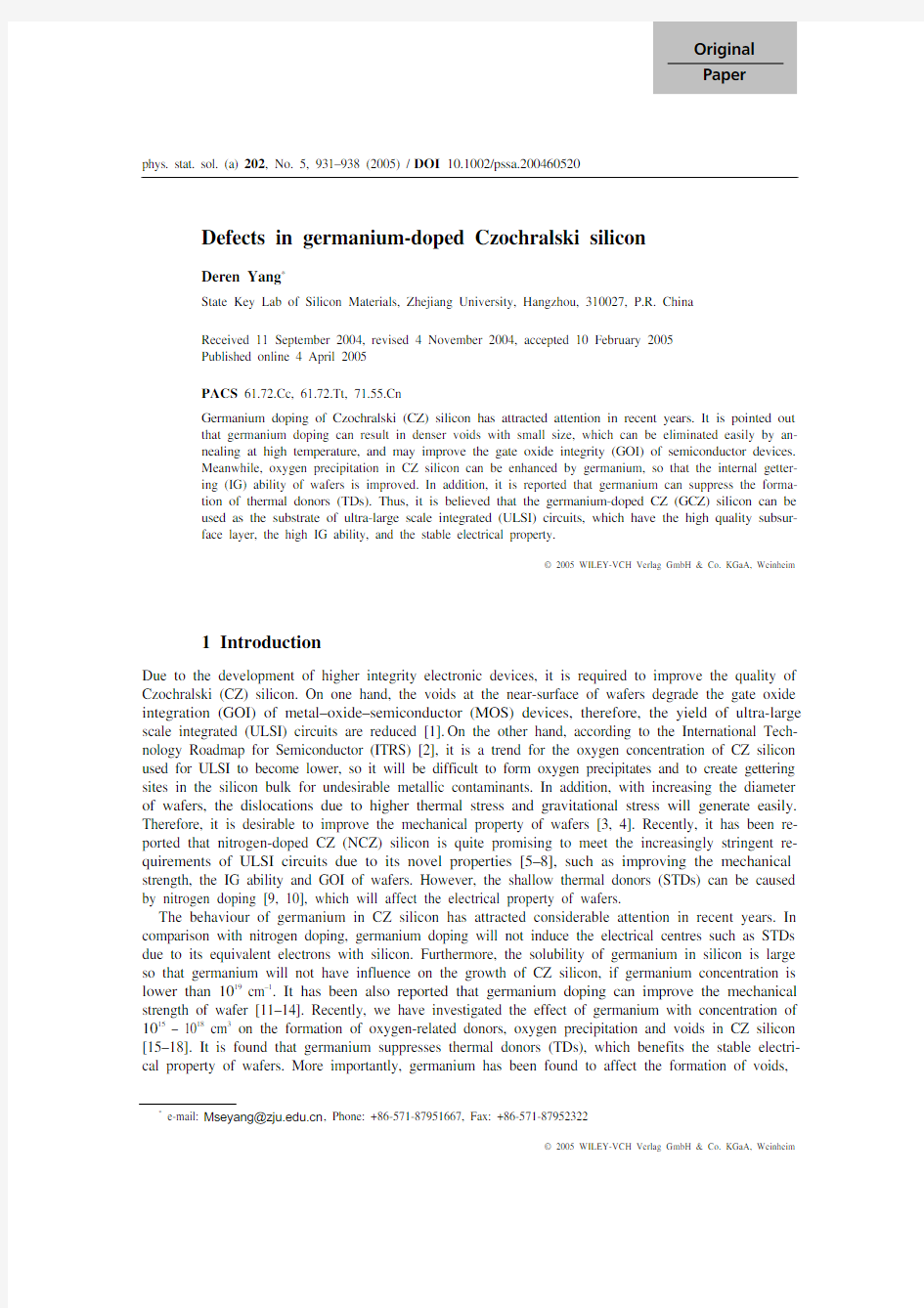
Fig. 1 TD (a) and ND (b) concentration in the CZ and GCZ wafers annealed at different temperature as a function of the annealing time. (a) 450 °C, (b) 650 °C.
which benefits for the easy elimination of voids at high temperature. Meanwhile, the enhancement of oxygen precipitation can be obtained by germanium doping and the IG ability is improved. In this article, these results based on our experiments about the germanium-doped CZ (GCZ) silicon have been re-viewed in detail.
2 Effect of germanium on oxygen-related donors
Oxygen atoms in CZ silicon is inclined to agglomerate to form oxygen-related donors included the TDs and NDs during crystal cooling or the thermal cycles of device fabrication, which can deteriorate the electrical stability of wafers. It is well known that the TDs generally form in the temperature range of 350 °C–550 °C [19, 20], while the NDs form in the temperature range of 550 °C–850 °C [21, 22].
In order to investigate the effect of germanium on the TD formation, the CZ and GCZ samples are annealed at 450 °C for different time. Figure 1(a) shows the TD concentration in the CZ and GCZ wafers as a function of the annealing time. It can be seen that the generation rate of TDs in the GCZ silicon was much lower than that in the CZ silicon, which clarifies that germanium doping suppresses the formation of TDs. Hild et al. have investigated TD formation at 450 °C in oxygen-rich SiGe with more than 1% Ge content and obtained also the similar results [23]. It is well known that TDs are small oxygen clusters. It is un-doubtful that during the formation of TDs, the lattice strain should be released by attracting free vacancies or ejecting interstitial silicon atoms into silicon matrix. Therefore, germanium atoms with the relative larger radius are inclined to complex with vacancies to form Ge–V complexes, which suppress the ejection of interstitial atoms, resulting in a retard of TD formation. On the other hand, the Ge–O complexes formation and their enhancement on oxygen precipitation will reduce the oxygen flux to form smaller oxygen clusters during lower temperature annealing, which also suppress the TD formation.
Regarding to the effect of germanium on ‘new donors’ (NDs), Babitski and co-workers have reported that germanium can suppress the formation of NDs [24]. However, here we will give an opposite result. Figure 1(b) shows the ND concentration in the CZ and GCZ wafers with the annealing time at 650 °C. It can be seen that the ND concentration in the GCZ silicon was much higher than that in the CZ silicon, which indicates that the huge number of the NDs generated due to the enhancement of germanium. The measurement results of the oxygen concentration show that the amount of oxygen precipitation in the GCZ silicon was much higher than that in the CZ silicon after the 650 °C/128 h annealing. So it can be concluded that more interstitial oxygen atoms have precipitated in the GCZ wafers than that in the CZ silicon during the formation of NDs, as a result of germanium enhancing on the nucleation of oxygen precipitates. It is well known that NDs are the bigger oxygen clusters compared to TDs, which can be-come the nuclei of oxygen precipitates [21, 22]. As germanium can enhance the nucleation of oxygen precipitates on the basis of the Ge–O complexes, some precipitate nuclei are believed to become the NDs. However, undoubtly, if germanium concentration in CZ silicon is much higher than oxygen con-centration, most of oxygen would be trapped by germanium to form Ge–O complexes, which results in
phys. stat. sol. (a) 202, No. 5 (2005) / https://www.sodocs.net/doc/5010017413.html, 933 ? 2005 WILEY-VCH Verlag GmbH & Co. KGaA, Weinheim
the decrease of oxygen flux to form NDs and the suppression of ND formation, as reported in Babitskii’s work [24].
3 Oxygen precipitation in GCZ silicon
3.1 Grown-in oxygen precipitation
It is well known that during crystal growth, grown-in oxygen precipitates can generate due to the post-annealing in crystal pullers. Generally, an annealing at considerably high temperature above 1250 °C can dissolve grown-in precipitates [7]. After the CZ and GCZ silicon were annealed at 1270 °C for 2 h, it is found that the ratio of increased [O i ] and as-received [O i ] was 1.9% in the CZ silicon, while 3.5% in the GCZ silicon, indicating the grow-in oxygen precipitates in the GCZ silicon was more than those in the CZ silicon. As the initial [O i ] and thermal history of the CZ and GCZ silicon was similar, it is considered that germanium enhanced the formation of the grown-in oxygen precipitates during crystal growth. If the CZ and GCZ silicon were cooled down by a rate of 0.5 °C/min after annealing at 1270 °C for 1 h, which annihilated the thermal history, the oxygen concentration decreased more rapidly in the GCZ silicon than in the CZ silicon. This result further clarifies that germanium can enhance oxygen precipitation during cooling process. Furthermore, it can be also found that germanium begin to enhance grown-in oxygen precipitation at above 1150 °C during crystal growth.
3.2 Thermal cycles
Figure 2(a) shows the [O i ]s in the CZ and GCZ silicon as a function of the annealing time at 800 °C and 1000 °C. It is obvious that more oxygen atoms precipitated in the GCZ in comparison with the CZ one. As can be seen, after 225 h annealing, the [O i ]s in the GCZ silicon reduced significantly to lower concen-trations. Furthermore, the bulk microdefect (BMD) density in the GCZ silicon was much higher than in the CZ silicon. Here, it should be mentioned that in the CZ silicon, during high temperature annealing such as 1000 °C, grown-in oxygen precipitates grew up easily by the aggregation of oxygen atoms while new homogenous nuclei of oxygen precipitates were difficult to generate. In general, only the grown-in oxygen precipitates of radius r larger than the critical radius r c at a certain annealing temperature can survive and grow up, while ones with r smaller than r c dissolve. So it can also be concluded that germa-nium enhances the formation of grown-in oxygen precipitates with larger size during crystal growth. Regarding to the enhancement of the oxygen precipitation in the GCZ silicon annealed at 800 °C, it is believed that germanium could enhance the nucleation of fresh oxygen precipitates at 800 °C. Figure 2(b) shows the microstructure of oxygen precipitates in the annealed CZ and GCZ samples. Generally, in the CZ silicon, plate-like precipitates are formed at intermediate temperatures (about 750 ~ 950 °C), and
[O i ](x 1017c m -3)Annealing Time (h)(a)200nm CZ/800o C 500nm GCZ/800o C 500nm
GCZ/1000o C CZ/1000o C (b)
Fig. 2 (a) [O i ]s in the CZ and GCZ silicon as a function of the annealing time at 800 °C and 1000 °C; (b) TEM images of the oxygen precipitates in the annealed CZ and GCZ silicon.
934 Deren Yang: Defects in germanium-doped Czochralski silicon ? 2005 WILEY-VCH Verlag GmbH & Co. KGaA, Weinheim
polyhedral ones at high temperatures (above 950 °C) [25, 26]. However, we found at 800 °C, the parti- cle-like precipitates besides platelet ones were generated in the GCZ silicon; meanwhile after 1000 °C/225 h annealing, the oxygen precipitates in the GCZ silicon were in mixed morphologies con-sisting of polyhedral and platelet. As a conclusion, it is believed that germanium doping changes the morphology of oxygen precipitates during annealing at different temperatures.
In the CZ and GCZ samples subjected to 1200 °C annealing following 800 °C/225 h or 1000 °C/225 h annealing, it is found that the [O i ]s increased much more larger in the GCZ samples than in the CZ sam-ples (see Fig. 3). The reason is that the quantity of the oxygen precipitates of radius smaller than r c at 1200 °C in the GCZ samples were much more than those in the CZ samples. In terms of the size, the oxygen precipitates formed during the prior annealing in both the CZ and GCZ samples were certainly not uniform. They could be classified into the two parts: one is whose sizes were below the r c for oxygen precipitate at 1200 °C, the other is reverse. Obviously, during the 1200 °C annealing, the oxygen precipi-tates whose sizes were larger than the r c would continuously grow up, while those smaller than the r c would be substantially dissolved. As we know, the growth or dissolution of oxygen precipitates is actually the oxygen flowing into or out of oxygen precipitates. When the formula D (C ox –C eq ) is positive, growth occurs; and when negative, dissolution occurs (D : oxygen diffusivity; C ox : actual oxygen concentration; C eq : oxygen solubility) [27]. In view of this point, it is understandable that in the CZ and GCZ silicon with the prior 800 °C, 1000 °C/225 h annealing the oxygen concentration increased significantly as a result of the nega-tive net oxygen flux out of oxygen precipitates in the early stages of the 1200 °C annealing, and afterwards decreased slightly due to the positive net oxygen flux into oxygen precipitates. However, for the GCZ sili-con with prior 1000 °C/225 h annealing, it is somewhat unexpected that the oxygen concentration increased during the 1200 °C annealing for up to 4 h, indicating that the dissolution of the oxygen precipitates sus-tained for quite a long time. In the previous work of Shimura et al. [27], it has been reported that oxygen precipitates formed in a prior 1000 °C annealing dissolved much more slowly than in a prior 750 °C anneal-ing. In general, the total surface area of oxygen precipitates is considered as the main reason that will de-termine the dissolution rate of oxygen precipitates. Thus, in the GCZ wafers, the oxygen precipitates with the larger size formed in the prior 1000 °C annealing would dissolute at a lower rate in comparison with those with the smaller size formed in the prior 800 °C annealing.
3.3 Effect mechanism of germanium on oxygen precipitation
It has been well known that the germanium atoms are located in substitutional position of silicon lattice. During the solidification of CZ silicon crystal, the substitutional germanium atoms will cause a lattice distortion [29], because the radius of Ge atom is larger than that of Si atom. To relieve the lattice stress, the germanium atoms incline to react with vacancies and further with interstitial oxygen to form related complexes, such as GeVO [15, 16], which can be illustrated by the reaction as follows,
Ge + V + O GeVO . (1)
[O i ](x 1017/c m 3)Annealing Time (h)
Fig. 3 [O i ]s in the CZ and GCZ silicon subjected to 1200 °C annealing following 800 °C/225 h or 1000 °C/225 h annealing.
phys. stat. sol. (a) 202, No. 5 (2005) / https://www.sodocs.net/doc/5010017413.html, 935 ? 2005 WILEY-VCH Verlag GmbH & Co. KGaA, Weinheim
At high temperatures before void formation, the concentration of free vacancies is higher, so the above reaction favors to the generation of GeVO complexes. The GeVO complexes can become the nuclei of oxygen precipitates by trapping more oxygen atoms and enhance oxygen precipitation in high tempera-ture range. After vacancies are consumed by void formation, the GeVO complexes cannot produce any more. Below the temperature of void formation, the germanium atoms are believed to directly bind oxy-gen to form GeO complexes via the reaction as below,
Ge + O GeO . (2) The GeO complexes can also trap more oxygen atoms to form the nuclei of oxygen precipitation, which enhance the formation of oxygen precipitates with smaller size.
4 Effect of germanium on voids
It has been reported that the voids, which are octahedral surrounded by {111} surfaces with a few nano-meter oxide films, are formed by aggregation of excess vacancies during crystal growth and have been known to degrade gate oxide integrity (GOI) of ULSI. After the SC1 or Secco etching, voids appeared on the wafer are called crystal originated particles (COPs) or flow pattern defects (FPDs), respectively [30, 31]. However, it should be mentioned that the density of FPDs is generally one order of magnitude lower than that of voids [30], because FPDs is believed only to represent the voids with larger size.
4.1 FPDs in GCZ silicon
Figure 4(a) shows the FPD densities in the as-grown CZ silicon and the GCZ silicon with the different germanium concentrations of 1015–1018/cm 3. It can be seen that for the seed-end samples, in which the germanium concentration was about 1017/cm 3, the FPD density was only about 9 × 10⁴/cm 3, much lower than that in the other corresponding samples. For the CZ silicon crystal, the FPD density of the tail sam-ple was almost the same as that of the seed-end sample. However, for the GCZ silicon crystals, the FPD density of the tail samples was lower than those of the head samples. Furthermore, the FPD densities of the tail samples of the GCZ silicon decreased with increasing germanium concentration. Accordingly, it can be concluded that germanium doping can significantly suppress voids with large size during crystal growth.
The CZ silicon and the GCZ silicon with the 1015/cm 3 of germanium, in which the FPD density was similar, were subjected to annealing at 1050 °C ~1200 °C for 2 or 4 h. The FPD density with the anneal-ing temperature is shown in Fig. 4(b). It can be seen that after annealing at 1050 °C only for 2 h, the FPD density in the GCZ silicon reduced significantly, while that in the CZ silicon almost kept constant. Although the FPD density in the CZ silicon decreased to considerable extent after 1150 °C annealing, it was still higher than that in the GCZ silicon. However, after annealing at 1200 °C, the FPD densities in
F P D d e n s i t y (×105/c m 3)Head segment Tail segment (a)F P D d e n s i t y (×105/c m 3)Temperature (°C )
Fig. 4 FPD densities in the CZ silicon and the GCZ silicon with the different germanium concentrations
of 1015–1018/cm 3 before (a) and after (b) annealing.
936
Deren Yang: Defects in germanium-doped Czochralski silicon ? 2005 WILEY-VCH Verlag GmbH & Co. KGaA, Weinheim
100
2003004000.11~0.120.12~0.130.13~0.180.18~0.25C O P n u m b e r (/w a f e r )Size(um)0
1002003000.11~0.120.12~0.130.13~0.180.18~0.25C O P n u m b e r (/w a f e r )Size(um)(a)
(b)
Fig. 5 Density and size profiles of the COPs on the CZ (a) and GCZ (b) silicon wafers.
both the CZ and GCZ silicon decreased to nearly the same level. It should be pointed out that the pro-longed annealing at high temperatures has no notable effect on the annihilation of FPDs because the FPD densities in the samples annealed for 2 h and 4 h at a given temperature only have slight distinction. From above facts, it can be concluded that the FPDs in the GCZ silicon can be annihilated at lower tem-perature, as compared with those in the CZ silicon, which implies that the thermal stability of the voids in the GCZ silicon is poorer.
4.2 COPs in GCZ silicon
The density and size profiles of the grown-in COPs in the CZ and GCZ wafers cut from the tail portion of crystals are shown in Fig. 5. It is obvious that the incorporation of germanium could enhance the den-sity of COPs and changed the size profile. It can be seen that in comparison with the CZ wafers, the percentage of COPs with the smaller size of 0.11 ~ 0.12 μm was higher on the GCZ wafers, and those with the larger size of over 0.12 μm was lower. Therefore, it is believed that germanium doping could induce denser COPs with smaller size.
After the CZ and GCZ silicon crystals were annealed in hydrogen atmosphere at the temperature of 1050 °C, 1150 °C and 1200 °C, respectively, it can be found that comparison with the CZ wafers, the COPs on the GCZ wafers could be annihilated easily at lower temperatures, which further suggests that germanium doping reduces the thermal stability of voids.
4.3 Effect mechanism of germanium on voids
As above-mentioned, at high temperatures such as 1150 °C during crystal growth, germanium can com-plex with vacancies or/and oxygen to form GeV or GeVO complexes, which become the nuclei of oxy-gen precipitates. Therefore, prior to the nucleation of voids, the nuclei of oxygen precipitates can grow up by the rapid diffusion of oxygen and absorption of a considerable amount of vacancies. Accordingly, the survived vacancies contributing to the formation of voids during the subsequent cooling are reduced. As a result, on one hand, denser voids with smaller size can generate easily by germanium; on the other hand, the characteristic formation temperature of voids controlled by super-saturation of vacancies definitely decreases to some extent, consequently, the size of voids in GCZ silicon will decrease and have poorer thermal stability, so they can be eliminated more easily compared with the case of CZ silicon crystals. 5 The DZ-IG technology of GCZ silicon
As the quality of defect-free denude zone (DZ) close to wafer surfaces is increasingly important for de-vice yield, internal gettering (IG) processes have been widely used in microelectronic industry. However, the oxygen concentration of CZ silicon used for ULSI becomes lower, so it will be difficult to form oxy-gen precipitates and create gettering sites in the bulk silicon.
phys. stat. sol. (a) 202, No. 5 (2005) / https://www.sodocs.net/doc/5010017413.html, 937
? 2005 WILEY-VCH Verlag GmbH & Co. KGaA, Weinheim
Fig. 6 Optical images of the cross section of the CZ silicon (a) and the GCZ silicon (b) contained 1018/cm 3 of germanium after three-step annealing (1200 °C/2 h + 750 °C/16 h + 1050 °C/16 h).
For the silicon subjected to high-low-high three-step annealing, it was found that with the temperature increase of first-step annealing, the width of the DZ in the CZ and GCZ silicon increased, which was a result of the out-diffusion of oxygen. However, the DZ width of the GCZ silicon was slightly narrower than that of the conventional CZ sample. Furthermore, with the concentration increase of germanium, the DZ width became narrower and narrower, but was still larger than 10 μm. Figure 6 shows the optical images of the cross section of the CZ silicon and the GCZ silicon contained the 1018 cm 3 of germanium after three-step annealing (1200 °C/2 h + 750 °C/16 h + 1050 °C/16 h). It can be seen that the DZ in the GCZ silicon was narrower, but the bulk microdefect (BMD) density in the bulk was higher, compared to the CZ silicon. It was also found that the [O i ] in the GCZ silicon was much lower than that in the CZ silicon, as a result of germanium enhancing oxygen precipitation.
After one-step high temperature annealing, the optical images of the cross section of the CZ and GCZ silicon are shown in Fig. 7. As it can be seen, numerous BMDs existed in the GCZ silicon, whereas, there were scarcely BMDs in the CZ silicon. It has been proved that germanium doping enhances oxygen precipitation at high temperature. Meanwhile, due to the out-diffusion of oxygen, the oxygen precipita-tion is substantially suppressed in the near-surface of the wafer in the GCZ silicon. Here, it should be emphasized that germanium could enhance the out-diffusion of oxygen at high temperature [15]. There-fore, it seems that one-step annealing at elevated temperatures is feasible for the IG process of the GCZ silicon.
6 Conclusions
The tetravalent germanium atoms exist at substitutional sites in silicon after incorporating into the crystal during growth. At high temperature prior to the formation of voids, the large oxygen precipitates can be enhanced by germanium based on the assumed GeVO complexes, while below the formation tempera-ture of voids, the oxygen precipitates can be enhanced by the assumed GeO complexes. Therefore, on one hand, denser voids with smaller size generate by germanium doping, which can be eliminated easily at lower temperature; on the other hand, during thermal cycles, the density of oxygen precipitates in the
Fig. 7 Optical images of the cross section of the CZ (a) and GCZ (b) silicon after one-step high tempera-ture annealing.
938 Deren Yang: Defects in germanium-doped Czochralski silicon ? 2005 WILEY-VCH Verlag GmbH & Co. KGaA, Weinheim
GCZ silicon is much higher than that in the CZ silicon, which improves the IG ability of wafers. Mean-while, it is clarified that the platelet oxygen precipitates generates in the annealed GCZ silicon easily. In addition, it has also been reported that the germanium suppresses the formation of TDs, which benefits for the stable electrical property of wafers.
Acknowledgements The authors would like to thank the Natural Science Foundation of China (Grant Nos. 50032010, 60225010 and 90307010) and REDP for financial supports.
References
[1] M. Itsumi, M. Maeda, and T. Ueki, J. Appl. Phys. 84, 1241 (1998).
[2] The International Technology Roadmap for Semiconductors (ITRS), Semiconductor Industry Association
(SIA) (San Jose, CA, 1999).
[3] A. A. Wereszczak, A. S. Barnes, K. Breder, and S. Binapal, J. Mater. Sci. 11, 291 (2000).
[4] M. Akatsuka, K. Sueoka, N. Adachi, N. Morimoto, and H. Katahama, Microelectron. Eng. 56, 99 (2001).
[5] D. Li, D. Yang, and D. Que, Physica B 273–274, 553 (1999).
[6] X. Yu, D. Yang, X. Ma, J. Yang, L. Li, and D. Que, J. Appl. Phys. 92, 188 (2002).
[7] X. Yu, D. Yang, X. Ma, L. Li, and D. Que, Semicond. Sci. Tech. 18, 399 (2003).
[8] X. Ma, X. Yu, R. Fan, and D. Yang, Appl. Phys. Lett. 81, 496 (2002).
[9] D. Yang, R. Fan, L. Li, and D. Que, Appl. Phys. Lett. 68, 487 (1996).
[10] D. Yang, D. Que, and K. Sumino, phys. stat. sol. (b) 210, 295 (1998).
[11] I. Yonenaga, T. Taishi, X. Huang, and K. Hoshikawa, J. Appl. Phys. 93, 265 (2003).
[12] T. Fukuda and A. Ohsawa, Appl. Phys. Lett. 60, 1184 (1992).
[13] W. P. Dumke and G. R. Woolhouse, IBM Tech. Discl. Bull. 21, 4687 (1979).
[14] T. Taishi, X. Huang, I. Yonenaga, and K. Hoshikawa, Mater. Sci. Semicond. Process. 5, 409 (2002).
[15] X. Yu, D. Yang, X. Ma, H. Li, Y. Shen, D. Tian, L. Li, and D. Que, J. Cryst. Growth 250, 359 (2003).
[16] D. Yang, X. Yu, X. Ma, J. Xu, L. Li, and D. Que, J. Cryst. Growth 243, 371 (2002).
[17] H. Li, D. Yang, X. Ma, X. Yu, and D. Que, J. Appl. Phys. 96, 4161 (2004).
[18] H. Li, D. Yang, X. Yu, X. Ma, and D. Que, J. Phys.: Condens. Matter 16, 5745 (2004).
[19] C. S. Fuller, N. B. Ditzenberger, N. B. Hannay, and E. Buchier, Phys. Rev. 96, 833 (1954).
[20] C. S. Fuller and R. A. Logan, J. Appl. Phys. 28, 1427 (1957).
[21] P. Capper, A. W. Jones, E. J. Wallhouse, and J. O. Wilkes, J. Appl. Phys. 48, 1646 (1977).
[22] B. Goldsmith, L. Jastrzebski, and R. Soyden, in: Defects in Silicon, edited by W. M. Bullis and L. C. Kimerling
(The Electrochemical Society, Pennington, NJ, 1983) p. 142.
[23] E. Hild, P. Gaworzewski, M. Franz, and K. Pressel, Appl. Phys. Lett. 72, 1362 (1998).
[24] U. Babitski, P. Grinshtaine, M. Ilin, M. Milvidski, and V. Kuznetsov, Phys. Tech. Semicond. 19, 982 (1985).
[25] A. Borghesi, B. Pivac, A. Sassella, and A. Stella, J. Appl. Phys. 77, 4169 (1995).
[26] K. Sueoka, N. Ikeda, T.Yamamoto, and S. Kobayashi, J. Appl. Phys. 74, 5437 (1993).
[27] F. Shimura, Oxygen in Silicon, Semicond. Semimetals 42, 367 (1994).
[28] A. Sassella, A. Borghesi, G. Borionetti, and P. Geranzani, Appl. Phys. Lett. 75, 1131 (1999).
[29] P. Dold, A. Barz, S. Recha, K. Pressel, M. Franz, and K. W. Benz, J. Cryst. Growth 192, 125 (1998).
[30] H. Yamagishi, I. Fusegawa, and N. Fujimaki, Semicond. Sci. Technol. 7, A135 (1992).
[31] J. Ryuta, E. Morita, T. Tanaka, and Y. Shimanuki, Jpn. J. Appl. Phys. 29, L1947 (1990).
广东单晶硅项目可行性分析报告
广东单晶硅项目可行性分析报告 规划设计/投资分析/产业运营
广东单晶硅项目可行性分析报告 单晶硅产品自2015年开始逐步扩大市场份额。近年来,单晶组件在我 国光伏组件出口总量中所占比例逐渐增加的趋势开始得到遏制,目前单晶 多晶出口比例基本维持在6:4的比例,单晶组件仍占据大部分市场份额。 从主要出口目的地国家的角度来看,出口日本、荷兰、澳大利亚的光伏组 件以单晶居多,这些国家更偏向高效组件产品,我国单晶出口比例的上升 与荷兰市场的开辟有着直接关系。巴西、印度则具有价格导向型市场的特征,以多晶组件占据大多数。 该单晶硅棒项目计划总投资6282.05万元,其中:固定资产投资 4748.56万元,占项目总投资的75.59%;流动资金1533.49万元,占项目 总投资的24.41%。 达产年营业收入14483.00万元,总成本费用11520.10万元,税金及 附加124.39万元,利润总额2962.90万元,利税总额3495.97万元,税后 净利润2222.18万元,达产年纳税总额1273.80万元;达产年投资利润率47.16%,投资利税率55.65%,投资回报率35.37%,全部投资回收期4.33年,提供就业职位285个。 坚持“实事求是”原则。项目承办单位的管理决策层要以求实、科学 的态度,严格按国家《建设项目经济评价方法与参数》(第三版)的要求,
在全面完成调查研究基础上,进行细致的论证和比较,做到技术先进、可靠、经济合理,为投资决策提供可靠的依据,同时,以客观公正立场、科 学严谨的态度对项目的经济效益做出科学的评价。 ...... 进入21世纪以来,全球单晶硅片行业的发展经历了兴盛(2007年以前)——低迷(2008-2016年底)——逐渐复苏(2017年以来)。兴盛期间, 行业市场规模曾经超过120亿美元。低迷时期,下游需求不振,市场供过 于求,导致单晶硅片价格屡屡下滑,行业规模不断下降,2009年达到了67 亿美元的低值,且本已进入众多企业研发范畴的18英寸单晶硅片技术也因 此而搁浅。直到2016年,全球单晶硅片行业仍未走出低迷状态,年销售额 仅72亿美元左右。
单晶硅行业分析报告
单晶硅行业分析报告 1、单晶硅分为半导体级和太阳能级两种,半导体级单晶硅是电子信息材料中最基础的材料,主要用于制造半导体和集成电路,太阳能级多晶硅主要用于制造太阳能电池。 2、日本、美国和德国是世界上硅材料的主要生产国,我国硅材料和日本同时起步,但技术较国际先进水平差距较大。目前国内企业主流产品为3”—6”硅片,而国际主流产品则为8”—12”硅片,且正在向12”硅片靠拢。 3、目前半导体单晶硅高端技术主要被几家国际大公司垄断,日本的信越公司、SUMCO公司、德国的WACKER公司和美国的MEMC等大型跨国企业占据了半导体单晶和硅片市场的90%。国内企业发展单晶硅面临技术和资金两大瓶颈,但我国太阳能级多晶硅技术接近国际先进水平,生产产量和出口额排名世界第一。 4、从市场供应状况看,全球和国内3”--6”电子级单晶硅片市场基本趋于饱和,受原材料市场影响基本没有利润空间,大尺寸单晶硅片市场需求增长迅猛,利润非常可观,已基本成为市场主流产品。太阳能级单晶硅今年呈高速增长趋势,但国内外的产能也在不断扩大,供需基本平衡。 5、全球太阳能多晶硅制造技术由发达国家的七家公司垄断,这七家公司占全球90%以上的市场份额。近两年,我国太阳能级多晶硅行业发展可谓突飞猛进,许多上规模的项目纷纷投产,从2008年起太阳能级多晶硅市场基本趋于供需平衡,到2008年下半年,伴随世界金融危机的蔓延,太阳能级多晶硅市场又面临严重的半停顿状态,价格快速回落,而且是有价无市。但电子级单晶硅技术由于被世界几大厂商垄断,国内仅有新光硅业一家能生产,供需矛盾非常突出,未来价格会居高不下。 6、单晶硅下游半导体器件市场一直呈平稳增长趋势,随着规律性起伏,也会产生一些调整,但总体增长趋势不变。而2005-2008年,太阳能市场呈爆发型市场增长态势,因此,市场对太阳能级多晶硅及单晶硅的需求较为旺盛。而半导
建筑工程施工质量缺陷案例及事故案例分析
建筑工程施工质量缺陷案例及事故案例分析 文件编码(008-TTIG-UTITD-GKBTT-PUUTI-WYTUI-8256)
建筑工程施工质量缺陷案例及事故案例分析 ======单选题部分====== 1.在主体结构工程施工中,当现场出现结构板双层双向钢筋的上层钢筋下陷的问题时,我们的处理建议是(C ) 2.室内墙地面饰面工程施工时,现场出现内墙大面空鼓裂纹问题的原因是() 3.以下不属于混凝土配合比直接决定的是() 4.碱骨料反应是混凝土原材料中的水泥、外加剂、混合材和水中的碱(Na2O 或K2O)与()中的活性成分反应,在混凝土浇筑成型后若干午(数年至二、三十年)逐渐反应,反应生成物吸水膨胀使混凝土产生内部应力,膨胀开裂、导致混凝土失去设计性能 ======多选题部分====== 5.以下属于外墙面工程施工时出现的现场问题的是() 6.预留预埋应按设计图纸要求事先翻样制作,并注明(),在浇筑混凝土前对模板的加固进行检查,保证拆模后预留预埋位置的准确,浇筑后及时复测,出现偏差及时调整 7.防水工程包括() ======判断题部分====== 8.屋面工程施工中,现场出现屋面顺水条间距未满足规定要求;屋面平整度差,引起局部用多根小木方支垫的问题时,我们的处理建议加强过程控制,确保每道施工程序按规范标准施工。(顺水条间距按照绿城规定执行)
9.滑模施工时应随时采用仪器或吊锤法检查滑升体系的垂直、扭转、倾斜等状态,对其结构的中心和边缘均应同步观察。 10.模板决定了混凝土构件的尺寸和观感,在支设模板前应进行研究和策划形成模板专项施工方案,并报工程管理科审批
单晶硅与多晶硅的区别、功能及优缺点
单晶硅与多晶硅的区别、功能及优缺点 单晶硅 硅有晶态和无定形两种同素异形体。晶态硅又分为单晶硅和多晶硅,它们均具有金刚石晶格,晶体硬而脆,具有金属光泽,能导电,但导电率不及金属,且随温度升高而增加,具有半导体性质。 单晶硅在日常生活中是电子计算机、自动控制系统等现代科学技术中不可缺少的基本材料。电视、电脑、冰箱、电话、手表、汽车,处处都离不开单晶硅材料,单晶硅作为科技应用普及材料之一,已经渗透到人们生活中的各个角落。 单晶硅在火星上是火星探测器中太阳能转换器的制成材料。火星探测器在火星上的能量全部来自太阳光,探测器白天休息---利用太阳能电池板把光能转化为电能存储起来,晚上则进行科学研究活动。也就是说,只要有了单晶硅,在太阳光照到的地方,就有了能量来源单晶硅在太空中是航天飞机、宇宙飞船、人造卫星必不可少的原材料。人类在征服宇宙的征途上,所取得的每一步进步,都有着单晶硅的身影。航天器材大部分的零部件都要以单晶硅为基础。离开单晶硅,卫星会没有能源,没有单晶硅,航天飞机和宇航员不会和地球取得联系,单晶硅作为人类科技进步的基石,为人类征服太空作出了不可磨灭的贡献。 单晶硅在太阳能电池中得到广泛的应用。高纯的单晶硅是重要的半导体材料,在光伏技术和微小型半导体逆变器技术飞速发展的今天,利用硅单晶所生产的太阳能电池可以直接把太阳能转化为光能,实现了迈向绿色能源革命的开始。单晶硅太阳能电池的特点:1.光电转换效率高,可靠性高; 2.先进的扩散技术,保证片内各处转换效率的均匀性; 3.运用先进的PECVD成膜技术,在电池表面镀上深蓝色的氮化硅减反射膜,颜色均匀美观;4.应用高品质的金属浆料制作背场和电极,确保良好的导电性。 单晶硅广阔的应用领域和良好的发展前景北京2008年奥运会将把"绿色奥运"做为重要展示面向全世界展现,单晶硅的利用在其中将是非常重要的一环。现在,国外的太阳能光伏电站已经到了理论成熟阶段,正在向实际应用阶段过渡,太阳能硅单晶的利用将是普及到全世界范围,市场需求量不言而喻。
硅单晶中晶体缺陷的腐蚀显示
硅单晶中晶体缺陷的腐蚀显示 实验安排:4人/组 时间:两小时 地点:北方工业大学第三教学楼2403房间 实验所用主要设备:金相显微镜 一、实验目的 硅单晶中的各种缺陷对器件的性能有很大的影响,它会造成扩散结面不平整,使晶体管中出现管道,引起p-n 结的反向漏电增大等。各种缺陷的产生和数量的多少与晶体制备工艺和器件工艺有关。晶体缺陷的实验观察方法有许多种,如透射电子显微镜、X光貌相技术、红外显微镜及金相腐蚀显示等方法。对表面缺陷也可以用扫描电子显微镜来观察。由于金相腐蚀显示技术设备简单,操作易掌握,又较直观,是观察研究晶体缺陷的最常用的方法之一。金相腐蚀显示可以揭示缺陷的数量和分布情况,找出缺陷形成、增殖和晶体制备工艺及器件工艺的关系,为改进工艺,减少缺陷、提高器件合格率和改善器件性能提供线索。 二、原理 硅单晶属金刚石结构,在实际的硅单晶中不可能整块晶体中原子完全按金刚石结构整齐排列,总又某些局部区域点阵排列的规律性被破坏,则该区域就称为晶体缺陷。硅单晶中的缺陷主要有点缺陷、线缺陷和面缺陷等三类。晶体缺陷可以在晶体生长过程中产生,也可以在热处理、晶体加工和受放射性辐射时产生。 在硅单晶中缺陷区不仅是高应力区,而且极易富集一些杂质,这样缺陷区就比晶格完整区化学活拨性强,对化学腐蚀剂的作用灵敏,因此容易被腐蚀而形成蚀坑,在有高度对称性的低指数面上蚀坑形状通常呈现相应的对称性,如位错在(111)、(100)、(110)面上分别呈三角形、方形和菱形蚀坑。 用作腐蚀显示的腐蚀剂按不同作用大体可分为两类,一类蚀非择优腐蚀剂,它主要用于晶体表面的化学抛光,目的在于达到清洁处理,去除机械损伤层和获得一个光亮的表面;另一类是择优腐蚀剂,用来揭示缺陷。一般腐蚀速度越快择择优性越差,而对择优腐蚀剂则要求缺陷蚀坑的出现率高、特征性强、再现性好和腐蚀时间短。 通常用的非择优腐蚀剂的配方为: HF(40-42%):HNO3(65%)=1:2.5 它们的化学反应过程为: Si+4HNO3+6HF=H2SiF6+4NO2+4H2O 通常用的择优腐蚀剂主要有以下二种: (1)希尔腐蚀液(铬酸腐蚀液) 先用CrO3与去离子水配成标准液: 标准液=50g CrO3+100g H2O 然后配成下列几种腐蚀液: A. 标准液:HF(40-42%)=2:1(慢速液) B. 标准液:HF(40-42%)=3:2(中速液) C. 标准液:HF(40-42%)=1:1(快速液) D. 标准液:HF(40-42%)=1:2(快速液) 一般常用的为配方C液,它们的化学反应过程为: Si+CrO3+8HF=H2SiF6+CrF2+3H2O (2)达希腐蚀液
建筑工程施工质量缺陷案例及事故案例分析审批稿
建筑工程施工质量缺陷 案例及事故案例分析 YKK standardization office【 YKK5AB- YKK08- YKK2C- YKK18】
建筑工程施工质量缺陷案例及事故案例分析 ======单选题部分====== ? 1.在主体结构工程施工中,当现场出现结构板双层双向钢筋的上层钢筋下陷的问题时,我们的处理建议是(C ) o?A 地下室顶板上需堆载施工时,必须明确设计使用荷载,均匀堆放施工材料,避免超载施工 o?B 在浇捣柱砼前,柱钢筋未作定位,钢筋无法与上层柱筋对齐,产生弯折 o?C 加强钢筋工程的阶段性验收及砼施工旁站控制 o?D 地下室后浇带大梁梁底无保护层,严重违反规范要求,影响梁使用寿命 ? 2.室内墙地面饰面工程施工时,现场出现内墙大面空鼓裂纹问题的原因是() o?A 商品砼坍落度过大,面层收缩形成裂纹 o?B 内墙粉刷砂浆配合比失控,强度很底,黄砂含泥量高且为细砂 o?C 外墙干挂石材收口于铝合金窗顶处,雨水渗入干挂石材空腔内流向窗顶部位,从窗顶薄弱处渗入室内 o?D 因房屋交付时,室内为毛坯,阳台进行地砖施工,室内外高度接近一致,阳、露台地砖为干粉砂浆铺贴,当雨水飘落到地面后从砖缝渗入干粉砂浆层,且阳、露台多为内坡,渗入雨水在干粉层内于墙根部位形成积水,积水沿砖墙渗入室内。 ? 3.以下不属于混凝土配合比直接决定的是() o?A 强度 o?B 和易性 o?C 经济性 o?D 坍落度 ? 4.碱骨料反应是混凝土原材料中的水泥、外加剂、混合材和水中的碱(Na2O或K2O)与()中的活性成分反应,在混凝土浇筑成型后若干午(数年至二、三十年)逐渐反应,反应生成物吸水膨胀使混凝土产生内部应力,膨胀开裂、导致混凝土失去设计性能 o?A 原料 o?B 骨料 o?C 水泥 o?D 水
无锡单晶硅项目投资分析报告
无锡单晶硅项目投资分析报告 规划设计/投资方案/产业运营
报告说明— 单晶硅产品自2015年开始逐步扩大市场份额。近年来,单晶组件在我国光伏组件出口总量中所占比例逐渐增加的趋势开始得到遏制,目前单晶多晶出口比例基本维持在6:4的比例,单晶组件仍占据大部分市场份额。从主要出口目的地国家的角度来看,出口日本、荷兰、澳大利亚的光伏组件以单晶居多,这些国家更偏向高效组件产品,我国单晶出口比例的上升与荷兰市场的开辟有着直接关系。巴西、印度则具有价格导向型市场的特征,以多晶组件占据大多数。 该单晶硅棒项目计划总投资13496.29万元,其中:固定资产投资11584.57万元,占项目总投资的85.84%;流动资金1911.72万元,占项目总投资的14.16%。 达产年营业收入14039.00万元,总成本费用11089.29万元,税金及附加225.42万元,利润总额2949.71万元,利税总额3581.99万元,税后净利润2212.28万元,达产年纳税总额1369.71万元;达产年投资利润率21.86%,投资利税率26.54%,投资回报率16.39%,全部投资回收期7.60年,提供就业职位303个。 从生产工艺来看,单多晶生产工艺差别主要体现在拉棒和铸锭环节,其中单晶硅棒工艺对设备、生产人员的要求严格,早期单晶硅片因长晶炉
投料量、生长速率、拉棒速度等方面技术不够成熟,生产成本居高不下,而多晶硅锭使用铸锭技术成本优势明显而占据主要市场份额。
目录 第一章概述 第二章项目建设单位 第三章项目建设必要性分析第四章项目市场调研 第五章建设规划 第六章项目选址可行性分析第七章项目工程方案分析第八章工艺说明 第九章项目环境影响分析第十章安全卫生 第十一章建设及运营风险分析第十二章项目节能方案分析第十三章实施安排 第十四章项目投资情况 第十五章经济效益 第十六章总结评价 第十七章项目招投标方案
单晶硅中可能出现的各种缺陷分析
单晶硅中可能出现的各种缺陷分析 缺陷,是对于晶体的周期性对称的破坏,使得实际的晶体偏离了理想晶体的晶体结构。在各种缺陷之中,有着多种分类方式,如果按照缺陷的维度,可以分为以下几种缺陷: 点缺陷:在晶体学中,点缺陷是指在三维尺度上都很小的,不超过几个原子直径的缺陷。其在三维尺寸均很小,只在某些位置发生,只影响邻近几个原子,有被称为零维缺陷。 线缺陷:线缺陷指二维尺度很小而们可以通过电镜等来对其进行观测。 面缺陷:面缺陷经常发生在两个不同相的界面上,或者同一晶体内部不同晶畴之间。界面两边都是周期排列点阵结构,而在界面处则出现了格点的错位。我们可以用光学显微镜观察面缺陷。 体缺陷:所谓体缺陷,是指在晶体中较大的尺寸范围内的晶格排列的不规则,比如包裹体、气泡、空洞等。 一、点缺陷 点缺陷包括空位、间隙原子和微缺陷等。 1、空位、间隙原子 点缺陷包括热点缺陷(本征点缺陷)和杂质点缺陷(非本征点缺陷)。 1.1热点缺陷 其中热点缺陷有两种基本形式:弗仑克尔缺陷和肖特基缺陷。单晶中空位和间隙原子在热平衡时的浓度与温度有关。温度愈高,平衡浓度愈大。高温生长
的硅单晶,在冷却过程中过饱和的间隙原子和空位要消失,其消失的途径是:空位和间隙原子相遇使复合消失;扩散到晶体表面消失;或扩散到位错区消失并引起位错攀移。间隙原子和空位目前尚无法观察。 1.2杂质点缺陷 A、替位杂质点缺陷,如硅晶体中的磷、硼、碳等杂质原子 B、间隙杂质点缺陷,如硅晶体中的氧等 1.3点缺陷之间相互作用 一个空位和一个间隙原子结合使空位和间隙原子同时湮灭(复合),两个空位形成双空位或空位团,间隙原子聚成团,热点缺陷和杂质点缺陷相互作用形成复杂的点缺陷复合体等。 2、微缺陷 2.1产生原因 如果晶体生长过程中冷却速度较快,饱和热点缺陷聚集或者他们与杂质的络合物凝聚而成间隙型位错环、位错环团及层错等。Cz硅单晶中的微缺陷,多数是各种形态的氧化物沉淀,它们是氧和碳等杂质,在晶体冷却过程中,通过均质成核和异质成核机理形成。 2.2微缺陷观察方法 1)择优化学腐蚀: 择优化学腐蚀后在横断面上呈均匀分布或组成各种形态的宏观漩涡花纹(漩涡缺陷)。宏观上,为一系列同心环或螺旋状的腐蚀图形,在显微镜下微缺陷的微观腐蚀形态为浅底腐蚀坑或腐蚀小丘(蝶形蚀坑)。在硅单晶的纵剖面上,微缺陷通常呈层状分布。 2)热氧化处理: 由于CZ硅单晶中的微缺陷,其应力场太小,往往需热氧化处理,使微缺陷缀饰长大或转化为氧化层错或小位错环后,才可用择优腐蚀方法显示。 3)扫描电子显微技术,X射线形貌技术,红外显微技术等方法。 2.3微缺陷结构
建筑工程施工质量缺陷案例及事故案例分析
建筑工程施工质量缺陷案例及事故案例分析 ======单选题部分====== ? 1.在主体结构工程施工中,当现场出现结构板双层双向钢筋的上层钢筋下陷的问题时,我们的处理建议是(C ) o A 地下室顶板上需堆载施工时,必须明确设计使用荷载,均匀堆放施工材料,避免超载施工 o B 在浇捣柱砼前,柱钢筋未作定位,钢筋无法与上层柱筋对齐,产生弯折 o C 加强钢筋工程的阶段性验收及砼施工旁站控制 o D 地下室后浇带大梁梁底无保护层,严重违反规范要求,影响梁使用寿命 ? 2.室内墙地面饰面工程施工时,现场出现内墙大面空鼓裂纹问题的原因是() o A 商品砼坍落度过大,面层收缩形成裂纹 o B 内墙粉刷砂浆配合比失控,强度很底,黄砂含泥量高且为细砂 o C 外墙干挂石材收口于铝合金窗顶处,雨水渗入干挂石材空腔内流向窗顶部位,从窗顶薄弱处渗入室内 o D 因房屋交付时,室内为毛坯,阳台进行地砖施工,室内外高度接近一致,阳、露台地砖为干粉砂浆铺贴,当雨水飘落到地面后从砖缝渗入干粉砂浆层,且阳、露台多为内坡,渗入雨水在干粉层内于墙根部位形成积水,积水沿砖墙渗入室内。 ? 3.以下不属于混凝土配合比直接决定的是() o A 强度 o B 和易性 o C 经济性 o D 坍落度 ? 4.碱骨料反应是混凝土原材料中的水泥、外加剂、混合材和水中的碱(Na2O或K2O)与()中的活性成分反应,在混凝土浇筑成型后若干午(数年至二、三十年)逐渐反应,反应生成物吸水膨胀使混凝土产生内部应力,膨胀开裂、导致混凝土失去设计性能 o A 原料 o B 骨料 o C 水泥 o D 水
======多选题部分====== ? 5.以下属于外墙面工程施工时出现的现场问题的是() o A 阳台外边梁上在进行室内装修后收口不合理,影响外观 o B 屋面露台防水未施工,墙面石材施工已完成,施工程序颠倒,墙根与屋面露台防水无法施工 o C 门厅前正面自由落水不合理 o D 窗顶装饰线两边出现大小头现象 ? 6.预留预埋应按设计图纸要求事先翻样制作,并注明(),在浇筑混凝土前对模板的加固进行检查,保证拆模后预留预埋位置的准确,浇筑后及时复测,出现偏差及时调整 o A 位置 o B 标高 o C 尺寸 o D 形状 ?7.防水工程包括() o A 地下室防水 o B 有防水要求的房间(如厨卫间) o C 屋面防水 o D 外墙的防渗漏 ======判断题部分====== ?8.屋面工程施工中,现场出现屋面顺水条间距未满足规定要求;屋面平整度差,引起局部用多根小木方支垫的问题时,我们的处理建议加强过程控制,确保每道施工程序按规范标准施工。(顺水条间距按照绿城规定执行) ?对错 ?9.滑模施工时应随时采用仪器或吊锤法检查滑升体系的垂直、扭转、倾斜等状态,对其结构的中心和边缘均应同步观察。 ?对错 ?10.模板决定了混凝土构件的尺寸和观感,在支设模板前应进行研究和策划形成模板专项施工方案,并报工程管理科审批 ?对错
山东单晶硅项目可行性分析报告
山东单晶硅项目可行性分析报告 规划设计/投资方案/产业运营
报告说明— 单晶硅产品自2015年开始逐步扩大市场份额。近年来,单晶组件在我国光伏组件出口总量中所占比例逐渐增加的趋势开始得到遏制,目前单晶多晶出口比例基本维持在6:4的比例,单晶组件仍占据大部分市场份额。从主要出口目的地国家的角度来看,出口日本、荷兰、澳大利亚的光伏组件以单晶居多,这些国家更偏向高效组件产品,我国单晶出口比例的上升与荷兰市场的开辟有着直接关系。巴西、印度则具有价格导向型市场的特征,以多晶组件占据大多数。 该单晶硅棒项目计划总投资9444.36万元,其中:固定资产投资7250.97万元,占项目总投资的76.78%;流动资金2193.39万元,占项目总投资的23.22%。 达产年营业收入20559.00万元,总成本费用16074.99万元,税金及附加190.73万元,利润总额4484.01万元,利税总额5293.22万元,税后净利润3363.01万元,达产年纳税总额1930.21万元;达产年投资利润率47.48%,投资利税率56.05%,投资回报率35.61%,全部投资回收期4.31年,提供就业职位381个。 从生产工艺来看,单多晶生产工艺差别主要体现在拉棒和铸锭环节,其中单晶硅棒工艺对设备、生产人员的要求严格,早期单晶硅片因长晶炉
投料量、生长速率、拉棒速度等方面技术不够成熟,生产成本居高不下,而多晶硅锭使用铸锭技术成本优势明显而占据主要市场份额。
目录 第一章概论 第二章项目建设单位基本情况第三章建设背景 第四章项目市场空间分析 第五章产品规划及建设规模第六章选址可行性分析 第七章土建工程设计 第八章工艺分析 第九章项目环保分析 第十章安全卫生 第十一章风险评估 第十二章节能说明 第十三章计划安排 第十四章投资计划方案 第十五章经济效益可行性 第十六章项目综合评估 第十七章项目招投标方案
第三节硅单晶
第三节硅单晶 一、直拉硅单晶 1961年1月,上海有色金属研究所第三研究室组建直拉硅单晶研制组,从制作设备开始,制成华东地区第一台直拉硅单晶炉。8月26日拉出1根重30克的硅单晶,受到复旦大学谢希德教授的称赞。11月又试制成掺磷、电阻率1~10欧姆·厘米的硅单晶。 [硅单晶] 1961年12月,上海金属加工厂在国产直筒式直拉硅单晶炉上试拉单晶,翌年2月拉制出重36克硅单晶,最初液态硅易结晶,成晶困难,在内层保温罩上加一层钼片,状况改观,电阻率均匀性也有提高。 1964年10月,为研制百万次电子计算机需要,上海市冶金工业局、市科学技术委员会联合向上海有色金属研究所下达研制生产电阻率为0.025~0.03欧姆·厘米的重掺硼硅单晶。该所第四研究室组成研制组,采用充氩工艺,完成了20个品种,供上海元件五厂制作11伏和37.5伏稳压管,经试用性能满足要求。翌年3月市冶金工业局邀请有关专家鉴定,确认工艺稳定,质量可靠,用多种方法掺杂均获得满意结果,并成功地验证了美国贝尔电话公司发表的电阻率曲线,填补了国内空白。国家科委以《重掺硼单晶的科学研究》为题,印成500本单行本内部发行。 随后该所又研制成硅外延衬底用电阻率为0.001~0.009欧姆·厘米重掺砷硅单晶和电阻率为0.003~0.009欧姆·厘米重掺锑硅单晶。经该所硅外延组和中国科学院上海冶金研究所长期使用,质量稳定可靠,是理想的硅外延衬底材料。市科委硅外延领导小组确认该成果填补了国内空白,要求除该所继续生产外,总结经验移交上海金属加工厂生产。1965年,该厂生产的硅单晶头部有滑移线、小角度晶界等缺陷,总工程师葛涛组织有关人员专题研究,总结经验教训,采取“引晶细长,放肩圆滑,直径均匀,尾呈圆锥”的16字经验。并延长停炉时间,缺陷得到改善,位错密度在5×10³个/平方厘米以下。1971年该厂在DJL-70硅单晶炉增加投料量试验,改进加热系统,扩大石墨器件尺寸,产量上升。1974年拉制出直径100毫米重5公斤硅单晶。为适应器件厂提高硅单晶的利用率的要求,1978年7月又首次拉制出符合质量要求的等直径硅单晶。 1970年,上海冶炼厂用直拉法制备硅单晶。为提高质量,1973年起采用偏心拉晶工艺,径向电阻率不均匀性小于20%,充氩减压工艺,降低氩气消耗
内蒙古单晶硅项目可行性分析报告
内蒙古单晶硅项目可行性分析报告 规划设计/投资分析/实施方案
报告说明— 进入21世纪以来,全球单晶硅片行业的发展经历了兴盛(2007年以前)——低迷(2008-2016年底)——逐渐复苏(2017年以来)。兴盛期间, 行业市场规模曾经超过120亿美元。低迷时期,下游需求不振,市场供过 于求,导致单晶硅片价格屡屡下滑,行业规模不断下降,2009年达到了67 亿美元的低值,且本已进入众多企业研发范畴的18英寸单晶硅片技术也因 此而搁浅。直到2016年,全球单晶硅片行业仍未走出低迷状态,年销售额 仅72亿美元左右。 该单晶硅棒项目计划总投资15285.88万元,其中:固定资产投资11867.07万元,占项目总投资的77.63%;流动资金3418.81万元,占项目 总投资的22.37%。 达产年营业收入24453.00万元,总成本费用19372.52万元,税金及 附加257.64万元,利润总额5080.48万元,利税总额6038.88万元,税后 净利润3810.36万元,达产年纳税总额2228.52万元;达产年投资利润率33.24%,投资利税率39.51%,投资回报率24.93%,全部投资回收期5.51年,提供就业职位466个。 单晶硅产品自2015年开始逐步扩大市场份额。近年来,单晶组件在我 国光伏组件出口总量中所占比例逐渐增加的趋势开始得到遏制,目前单晶 多晶出口比例基本维持在6:4的比例,单晶组件仍占据大部分市场份额。
从主要出口目的地国家的角度来看,出口日本、荷兰、澳大利亚的光伏组件以单晶居多,这些国家更偏向高效组件产品,我国单晶出口比例的上升与荷兰市场的开辟有着直接关系。巴西、印度则具有价格导向型市场的特征,以多晶组件占据大多数。
单晶硅中可能出现的各种缺陷
单晶硅中可能出现的各种缺陷 缺陷,是对于晶体的周期性对称的破坏,使得实际的晶体偏离了理想晶体的晶体结构。在各种缺陷之中,有着多种分类方式,如果按照缺陷的维度,可以分为以下几种缺陷:点缺陷:在晶体学中,点缺陷是指在三维尺度上都很小的,不超过几个原子直径的缺陷。其在三维尺寸均很小,只在某些位置发生,只影响邻近几个原子,有被称为零维缺陷。线缺陷:线缺陷指二维尺度很小而第三维尺度很大的缺陷,也就是位错。我们可以通过电镜等来对其进行观测。面缺陷:面缺陷经常发生在两个不同相的界面上,或者同一晶体内部不同晶畴之间。界面两边都是周期排列点阵结构,而在界面处则出现了格点的错位。我们可以用光学显微镜观察面缺陷。体缺陷:所谓体缺陷,是指在晶体中较大的尺寸范围内的晶格排列的不规则,比如包裹体、气泡、空洞等。 一、点缺陷点缺陷包括空位、间隙原子和微缺陷等。 1、空位、间隙原子点缺陷包括热点缺陷(本征点缺陷)和杂质点缺陷(非本征点缺陷)。 1.1热点缺陷其中热点缺陷有两种基本形式:弗仑克尔缺陷和肖特基缺陷。单晶中空位和间隙原子在热平衡时的浓度与温度有关。温度愈高,平衡浓度愈大。高温生长的硅单晶,在冷却过程中过饱
和的间隙原子和空位要消失,其消失的途径是:空位和间隙原子相遇使复合消失;扩散到晶体表面消失;或扩散到位错区消失并引起位错攀移。间隙原子和空位目前尚无法观察。 1.2杂质点缺陷A、替位杂质点缺陷,如硅晶体中的磷、硼、碳等杂质原子B、间隙杂质点缺陷,如硅晶体中的氧等 1.3点缺陷之间相互作用一个空位和一个间隙原子结合使空位和间隙原子同时湮灭(复合),两个空位形成双空位或空位团,间隙原子聚成团,热点缺陷和杂质点缺陷相互作用形成复杂的点缺陷复合体等。2、微缺陷 2.1产生原因如果晶体生长过程中冷却速度较快,饱和热点缺陷聚集或者他们与杂质的络合物凝聚而成间隙型位 错环、位错环团及层错等。Cz硅单晶中的微缺陷,多数是各种形态的氧化物沉淀,它们是氧和碳等杂质,在晶体冷却过程中,通过均质成核和异质成核机理形成。 2.2微缺陷观察方法1)择优化学腐蚀:择优化学腐蚀后在横断面上呈均匀分布或组成各种形态的宏观漩涡花纹(漩涡缺陷)。宏观上,为一系列同心环或螺旋状的腐蚀图形,在显微镜下微缺陷的微观腐蚀形态为浅底腐蚀坑或腐蚀小丘(蝶形蚀坑)。在硅单晶的纵剖面上,微缺陷通常呈层状分布。2)热氧化处理:由于CZ硅单晶中的微缺陷,其应力场太小,往往需热氧化处理,使微缺陷缀饰长大或转化为氧化层错或小位错环后,才可用择优腐蚀方法显示。3)扫
河南单晶硅项目实施方案投资分析报告
河南单晶硅项目 实施方案 规划设计/投资分析/实施方案
报告说明— 硅棒在2018年和2020年能分别达到1942万片/月和2130万片/月,预计2015年到2020年之间符合年均增速为5.4%。硅棒指的是作用主要是耐火耐高温材料,做高温发热的元件,为无色立方或六方晶体,表面氧化或含杂质时呈蓝黑色。 该单晶硅棒项目计划总投资15972.16万元,其中:固定资产投资11625.22万元,占项目总投资的72.78%;流动资金4346.94万元,占项目总投资的27.22%。 达产年营业收入31348.00万元,总成本费用24713.26万元,税金及附加290.57万元,利润总额6634.74万元,利税总额7840.45万元,税后净利润4976.06万元,达产年纳税总额2864.39万元;达产年投资利润率41.54%,投资利税率49.09%,投资回报率31.15%,全部投资回收期4.71年,提供就业职位495个。 从生产工艺来看,单多晶生产工艺差别主要体现在拉棒和铸锭环节,其中单晶硅棒工艺对设备、生产人员的要求严格,早期单晶硅片因长晶炉投料量、生长速率、拉棒速度等方面技术不够成熟,生产成本居高不下,而多晶硅锭使用铸锭技术成本优势明显而占据主要市场份额。
第一章项目概况 一、项目概况 (一)项目名称及背景 河南单晶硅项目 单晶硅产品自2015年开始逐步扩大市场份额。近年来,单晶组件在我 国光伏组件出口总量中所占比例逐渐增加的趋势开始得到遏制,目前单晶 多晶出口比例基本维持在6:4的比例,单晶组件仍占据大部分市场份额。 从主要出口目的地国家的角度来看,出口日本、荷兰、澳大利亚的光伏组 件以单晶居多,这些国家更偏向高效组件产品,我国单晶出口比例的上升 与荷兰市场的开辟有着直接关系。巴西、印度则具有价格导向型市场的特征,以多晶组件占据大多数。 进入21世纪以来,全球单晶硅片行业的发展经历了兴盛(2007年以前)——低迷(2008-2016年底)——逐渐复苏(2017年以来)。兴盛期间, 行业市场规模曾经超过120亿美元。低迷时期,下游需求不振,市场供过 于求,导致单晶硅片价格屡屡下滑,行业规模不断下降,2009年达到了67 亿美元的低值,且本已进入众多企业研发范畴的18英寸单晶硅片技术也因 此而搁浅。直到2016年,全球单晶硅片行业仍未走出低迷状态,年销售额 仅72亿美元左右。
建筑工程安全事故案例分析(正式)
编订:__________________ 单位:__________________ 时间:__________________ 建筑工程安全事故案例分 析(正式) Deploy The Objectives, Requirements And Methods To Make The Personnel In The Organization Operate According To The Established Standards And Reach The Expected Level. Word格式 / 完整 / 可编辑
文件编号:KG-AO-3235-90 建筑工程安全事故案例分析(正式) 使用备注:本文档可用在日常工作场景,通过对目的、要求、方式、方法、进度等进行具体、周密的部署,从而使得组织内人员按照既定标准、规范的要求进行操作,使日常工作或活动达到预期的水平。下载后就可自由编辑。 近年来,随着我国经济建设的蓬勃发展,建筑行业也得到了长足的进步,但是在飞速发展的同时,随之而来的各类建筑工程事故也是层出不穷,安全问题越来越成为我们建筑行业在工程建设中不可忽略的因素。 然而,造成建筑工程事故的原因最主要的两个方面就是建筑物本身质量低下和施工方的不合理操作,分析如下: 1、工程中的缺陷,是由人为的(勘察、设计、施工、建材使用)或自然的(地质、气候)原因,在建筑物的正常使用过程中出现的承载力、耐久力、整体稳定性的种种不足的统称。它按照严重程度不同,又可分为三类: (1)轻微缺陷。它们并不影响建筑物的近期使用,
也不影响建筑结构的承载力、刚度及其完整性,但却有碍观瞻或影响耐久性。例如地面不平整,地面混凝土龟裂,混凝土表面局部缺浆、起砂,钢板上划痕、夹渣等。 (2)使用缺陷。它们虽然不影响建筑结构的承载力。却影响建筑物的使用功能,或使结构的使用性能下降。有时候还会使人有不舒适和不安全感。大多是由于施工不合理和建筑材料使用不合理或者偷工减料造成的。例如屋面和地下室渗漏,装饰物受损,梁的挠度偏大,墙体因温度差出现斜向或竖向裂纹等。 (3)危及承载力缺陷。它们表现为采用材料的强度不足,或表现为结构件截面尺寸不够,或表现为连接构造质量低劣,例如混凝土振捣固实,配筋欠缺,钢结构焊缝有裂纹,咬边现象。地基发生过大的沉降速率等。这类缺陷威胁到结构的承载力和稳定性,如不及时消除。可能导致局部或整体的破坏。 三类缺陷可能是显露的,如屋面渗透;也可能是隐蔽的,如配筋不足,等等在隐蔽部位建筑材料使用
宁波单晶硅项目实施方案投资分析报告
宁波单晶硅项目 实施方案 规划设计/投资分析/实施方案
报告说明— 硅棒在2018年和2020年能分别达到1942万片/月和2130万片/月,预计2015年到2020年之间符合年均增速为5.4%。硅棒指的是作用主要是耐火耐高温材料,做高温发热的元件,为无色立方或六方晶体,表面氧化或含杂质时呈蓝黑色。 该单晶硅棒项目计划总投资9404.47万元,其中:固定资产投资6639.35万元,占项目总投资的70.60%;流动资金2765.12万元,占项目总投资的29.40%。 达产年营业收入23464.00万元,总成本费用18587.82万元,税金及附加183.32万元,利润总额4876.18万元,利税总额5732.08万元,税后净利润3657.14万元,达产年纳税总额2074.95万元;达产年投资利润率51.85%,投资利税率60.95%,投资回报率38.89%,全部投资回收期4.07年,提供就业职位379个。 从生产工艺来看,单多晶生产工艺差别主要体现在拉棒和铸锭环节,其中单晶硅棒工艺对设备、生产人员的要求严格,早期单晶硅片因长晶炉投料量、生长速率、拉棒速度等方面技术不够成熟,生产成本居高不下,而多晶硅锭使用铸锭技术成本优势明显而占据主要市场份额。
第一章概论 一、项目概况 (一)项目名称及背景 宁波单晶硅项目 单晶硅产品自2015年开始逐步扩大市场份额。近年来,单晶组件在我 国光伏组件出口总量中所占比例逐渐增加的趋势开始得到遏制,目前单晶 多晶出口比例基本维持在6:4的比例,单晶组件仍占据大部分市场份额。 从主要出口目的地国家的角度来看,出口日本、荷兰、澳大利亚的光伏组 件以单晶居多,这些国家更偏向高效组件产品,我国单晶出口比例的上升 与荷兰市场的开辟有着直接关系。巴西、印度则具有价格导向型市场的特征,以多晶组件占据大多数。 进入21世纪以来,全球单晶硅片行业的发展经历了兴盛(2007年以前)——低迷(2008-2016年底)——逐渐复苏(2017年以来)。兴盛期间, 行业市场规模曾经超过120亿美元。低迷时期,下游需求不振,市场供过 于求,导致单晶硅片价格屡屡下滑,行业规模不断下降,2009年达到了67 亿美元的低值,且本已进入众多企业研发范畴的18英寸单晶硅片技术也因 此而搁浅。直到2016年,全球单晶硅片行业仍未走出低迷状态,年销售额 仅72亿美元左右。
单晶硅棒项目可行性研究报告
单晶硅棒项目可行性研究报告 投资分析/实施方案
报告摘要说明 单晶硅产品自2015年开始逐步扩大市场份额。近年来,单晶组件在我 国光伏组件出口总量中所占比例逐渐增加的趋势开始得到遏制,目前单晶 多晶出口比例基本维持在6:4的比例,单晶组件仍占据大部分市场份额。 从主要出口目的地国家的角度来看,出口日本、荷兰、澳大利亚的光伏组 件以单晶居多,这些国家更偏向高效组件产品,我国单晶出口比例的上升 与荷兰市场的开辟有着直接关系。巴西、印度则具有价格导向型市场的特征,以多晶组件占据大多数。 进入21世纪以来,全球单晶硅片行业的发展经历了兴盛(2007年以前)——低迷(2008-2016年底)——逐渐复苏(2017年以来)。兴盛期间, 行业市场规模曾经超过120亿美元。低迷时期,下游需求不振,市场供过 于求,导致单晶硅片价格屡屡下滑,行业规模不断下降,2009年达到了67 亿美元的低值,且本已进入众多企业研发范畴的18英寸单晶硅片技术也因 此而搁浅。直到2016年,全球单晶硅片行业仍未走出低迷状态,年销售额 仅72亿美元左右。 该单晶硅棒项目计划总投资8599.78万元,其中:固定资产投资6103.55万元,占项目总投资的70.97%;流动资金2496.23万元,占 项目总投资的29.03%。
本期项目达产年营业收入19733.00万元,总成本费用15340.03 万元,税金及附加166.33万元,利润总额4392.97万元,利税总额5165.23万元,税后净利润3294.73万元,达产年纳税总额1870.50万元;达产年投资利润率51.08%,投资利税率60.06%,投资回报率38.31%,全部投资回收期4.11年,提供就业职位390个。 硅棒在2018年和2020年能分别达到1942万片/月和2130万片/月,预计2015年到2020年之间符合年均增速为5.4%。硅棒指的是作用主要是耐火耐高温材料,做高温发热的元件,为无色立方或六方晶体,表面氧化或含杂质时呈蓝黑色。 从生产工艺来看,单多晶生产工艺差别主要体现在拉棒和铸锭环节,其中单晶硅棒工艺对设备、生产人员的要求严格,早期单晶硅片因长晶炉投料量、生长速率、拉棒速度等方面技术不够成熟,生产成本居高不下,而多晶硅锭使用铸锭技术成本优势明显而占据主要市场份额。
金属热处理缺陷分析及案例
金属热处理缺陷分析及 案例 Document serial number【KKGB-LBS98YT-BS8CB-BSUT-BST108】
<<金属热处理缺陷分析及案例>>试题 一、填空题 1、热处理缺陷产生的原因是多方面的,概括起来可分为热处理前、热处理中、热处理后三个方面的原因。 2、热处理缺陷分析方法有:断口分析、化学分析、金相检验、力学性能试验、验证试验、综合分析。 3、断裂可分为两种类型:脆性断裂和韧性断裂。 4、金属断裂的理论研究表明:任何应力状态都可以用切应力和正应力表示,这两种应力对变形和断裂起着不同的作用,只有切应力才可以引起金属发生塑性变形,而正应力只影响断裂的发展过程。 5、热处理变形常用的校正方法可分为机械校正法和热处理校正法。 6、热应力是指由表层与心部的温度差引起的胀缩不均匀而产生的内应力。 7、工程上常用的表面淬火方法主要有高频感应加热淬火和火焰淬火两种。 8、热处理中质量控制的关键是控制加热质量和冷却质量。 9、过热组织晶粒粗大的主要特征是奥氏体晶粒度在3级以下。 10、真空热处理常见缺陷有表面合金元素贫化、表面不光亮和氧化色、表面增碳或增氮、粘连、淬火硬度不足、表面晶粒长大。 11、低温回火温度范围是(150-250)℃,中温回火温度范围是(350-500)℃,高温回火温度范围是(500-6 50)℃。
12、工件的形状愈不对称,或冷却的不均匀性愈大,淬火后的变形也愈明显。 13、马氏体片越长,撞击能量越高,显微裂纹密度会越大,撞击应力会越大,显微裂纹的数目和长度也会增加。 14、合金元素通过对淬透性的影响,从而影响到淬裂倾向,一般来说,淬透性增加,淬裂性会增加。合金元素对M S的影响较大,一般来说,M S越低的钢,淬裂倾向越大。 15、一般来说,形状简单的工件,可采用上限加热温度,形状复杂、易淬裂的工件,则应采用下限加热温度。 16、对于低碳钢制工件,若正常加热温度淬火后内孔收缩,为了减小收缩,要降低淬火加热温度;对于中碳合金钢制的工件,若正常加热温度淬火后内孔胀大,为了减小孔腔的胀大,需降低淬火加热温度。 17、工件的热处理变形分为尺寸变化和形状畸变两种形式。 二、单项选择题 1、淬火裂纹通常分为 A 四种。 A、纵向裂纹、横向裂纹、网状裂纹、剥离裂纹 B、纵向裂纹、横向裂纹、剥离裂纹、显微裂纹 C、纵向裂纹、横向裂纹、网状裂纹、表面裂纹 D、纵向裂纹、横向裂纹、剥离裂纹、应力集中裂纹 2、第一类回火脆性通常发生在淬火马氏体于 B 回火温度区间,这类回火脆性在碳钢和合金钢中均会出现,它与回火后的冷却速度无关。 A、(200-300)℃ B、(200-400)℃
东莞单晶硅项目可行性分析报告
东莞单晶硅项目可行性分析报告 规划设计/投资方案/产业运营
东莞单晶硅项目可行性分析报告 单晶硅产品自2015年开始逐步扩大市场份额。近年来,单晶组件在我国光伏组件出口总量中所占比例逐渐增加的趋势开始得到遏制,目前单晶多晶出口比例基本维持在6:4的比例,单晶组件仍占据大部分市场份额。从主要出口目的地国家的角度来看,出口日本、荷兰、澳大利亚的光伏组件以单晶居多,这些国家更偏向高效组件产品,我国单晶出口比例的上升与荷兰市场的开辟有着直接关系。巴西、印度则具有价格导向型市场的特征,以多晶组件占据大多数。 该单晶硅棒项目计划总投资6883.44万元,其中:固定资产投资5415.08万元,占项目总投资的78.67%;流动资金1468.36万元,占项目总投资的21.33%。 达产年营业收入10254.00万元,总成本费用7731.65万元,税金及附加125.34万元,利润总额2522.35万元,利税总额2995.60万元,税后净利润1891.76万元,达产年纳税总额1103.84万元;达产年投资利润率36.64%,投资利税率43.52%,投资回报率27.48%,全部投资回收期5.14年,提供就业职位150个。 坚持应用先进技术的原则。根据项目承办单位和项目建设地的实际情况,合理制定项目产品方案及工艺路线,在项目产品生产技术设计上充分
体现设备的技术先进性、操作安全性。采用先进适用的项目产品生产工艺 技术,努力提高项目产品生产装置自动化控制水平,以经济效益为中心, 在采用先进工艺和高效设备的同时,做好项目投资费用的控制工作,以求 实科学的态度进行细致的论证和比较,为投资决策提供可靠的依据。努力 提高项目承办单位的整体技术水平和装备水平,增强企业的整体经济实力,使企业完全进入可持续发展的境地。 ...... 进入21世纪以来,全球单晶硅片行业的发展经历了兴盛(2007年以前)——低迷(2008-2016年底)——逐渐复苏(2017年以来)。兴盛期间, 行业市场规模曾经超过120亿美元。低迷时期,下游需求不振,市场供过 于求,导致单晶硅片价格屡屡下滑,行业规模不断下降,2009年达到了67 亿美元的低值,且本已进入众多企业研发范畴的18英寸单晶硅片技术也因 此而搁浅。直到2016年,全球单晶硅片行业仍未走出低迷状态,年销售额 仅72亿美元左右。
相关文档
- 建筑工程施工质量缺陷案例与事故案例分析报告
- 建筑工程施工质量缺陷案例及事故案例分析
- 护理缺陷案例分析
- 施工现场存在问题案例分析
- 建筑工程施工质量缺陷案例及事故案例分析
- 建筑工程安全事故案例分析(正式)
- 建筑设计工程施工质量缺陷案例及事故案例分析.doc
- 装修工程常见缺陷案例集
- 房屋建筑工程缺陷案例分析经典.pptx
- 建筑工程施工质量缺陷案例及事故案例分析审批稿
- 金属热处理缺陷分析及案例
- 建筑工程施工质量缺陷案例及事故案例分析
- 建筑工程施工质量缺陷案例及事故案例分析
- 建筑工程施工质量缺陷案例及事故案例分析.doc
- 高大模板支撑施工常见问题案例分析
- 房屋建筑工程缺陷案例分析
- 常见工程质量案例分析教学文案
- 建筑工程施工质量缺陷案例及事故案例分析
- 工程监理案例分析案例知识分享
- Removed_室外配套工程质量通病案例分析