MAX6174AASA-T中文资料

General Description
The MAX6173–MAX6177 are low-noise, high-precision voltage references. The devices feature a proprietary temperature-coefficient curvature-correction circuit and laser-trimmed thin-film resistors that result in a very low 3ppm/°C temperature coefficient and excellent ±0.06%initial accuracy. The MAX6173–MAX6177 provide a TEMP output where the output voltage is proportional to the die temperature, making the devices suitable for a wide variety of temperature-sensing applications. The devices also provide a TRIM input, allowing fine trimming of the output voltage with a resistive divider network. Low temperature drift and low noise make the devices ideal for use with high-resolution A/D or D/A converters.
The MAX6173–MAX6177 provide accurate preset +2.5V,+3.3V, +4.096V, +5.0V, and +10V reference voltages and accept input voltages up to +40V. The devices draw 320μA (typ) of supply current and source 30mA or sink 2mA of load current. The MAX6173–MAX6177 use bandgap technology for low-noise performance and excellent accuracy. The MAX6173–MAX6177 do not require an output bypass capacitor for stability, and are stable with capacitive loads up to 100μF. Eliminating the output bypass capacitor saves valuable board area in space-critical applications.
The MAX6173–MAX6177 are available in an 8-pin SO package and operate over the automotive (-40°C to +125°C) temperature range.
Applications
A/D Converters Voltage Regulators D/A Converters Threshold Detectors
Digital Voltmeters
Features
?Wide (V OUT + 2V) to +40V Supply Voltage Range ?Excellent Temperature Stability: 3ppm/°C (max)?Tight Initial Accuracy: 0.05% (max)?Low Noise: 3.8μV P-P (typ at 2.5V Output)?Sources up to 30mA Output Current ?Low Supply Current: 450μA (max at +25°C)?Linear Temperature Transducer Voltage Output ?+2.5V, +3.3V, +4.096V, +5.0V, or +10V Output Voltages ?Wide Operating Temperature Range: -40°C to +125°C ?No External Capacitors Required for Stability ?Short-Circuit Protected
MAX6173–MAX6177
High-Precision Voltage References with
Temperature Sensor
________________________________________________________________Maxim Integrated Products 1
19-3249; Rev 0; 5/04
For pricing, delivery, and ordering information,please contact Maxim/Dallas Direct!at 1-888-629-4642, or visit Maxim’s website at https://www.sodocs.net/doc/5a18239472.html,.
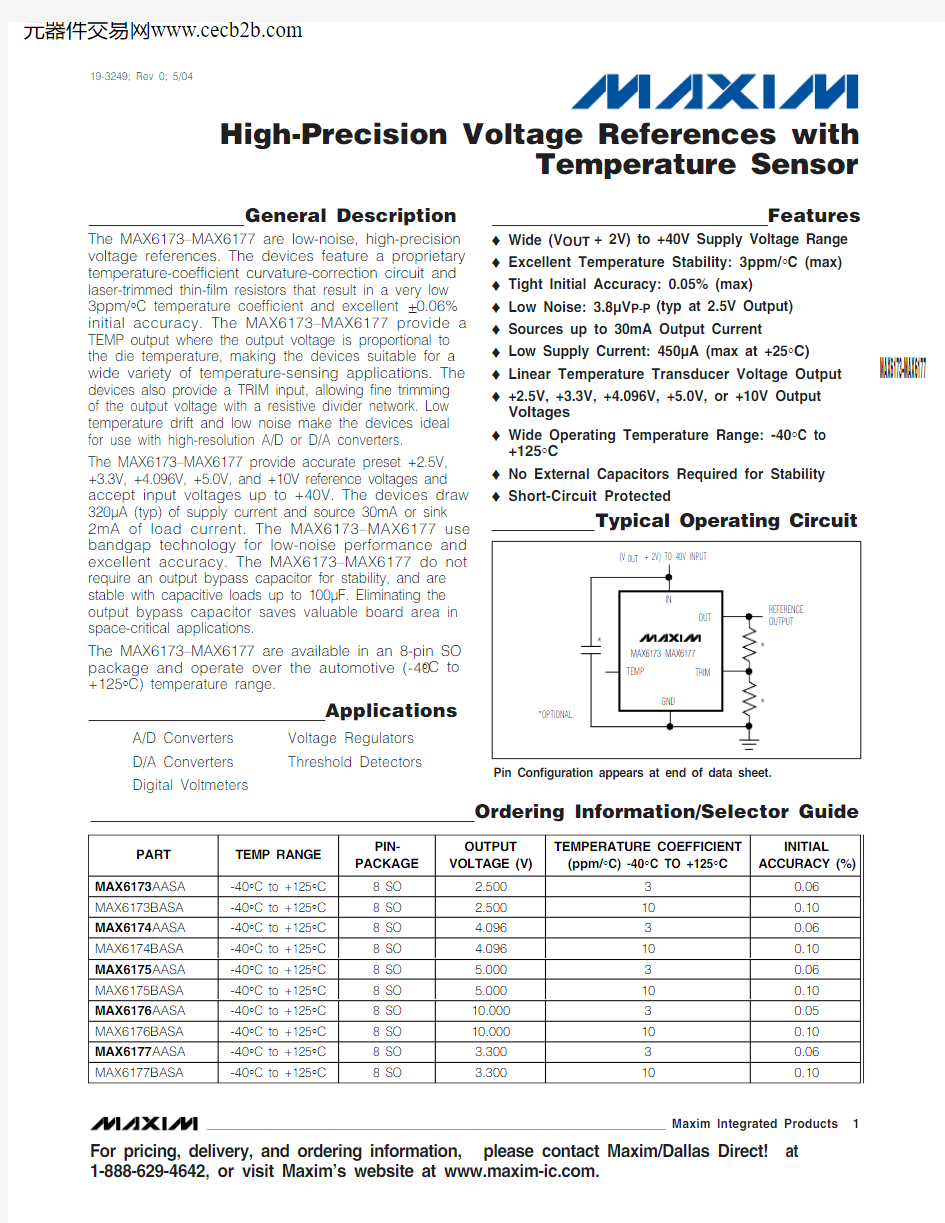
Pin Configuration appears at end of data sheet.
Ordering Information/Selector Guide
Typical Operating Circuit
M A X 6173–M A X 6177
High-Precision Voltage References with Temperature Sensor
ABSOLUTE MAXIMUM RATINGS
Stresses beyond those listed under “Absolute Maximum Ratings” may cause permanent damage to the device. These are stress ratings only, and functional operation of the device at these or any other conditions beyond those indicated in the operational sections of the specifications is not implied. Exposure to absolute maximum rating conditions for extended periods may affect device reliability.
IN to GND...............................................................-0.3V to +42V OUT, TRIM, TEMP to GND...........................-0.3V to (V IN + 0.3V)Output Short Circuit to GND.....................................................5s Continuous Power Dissipation (T A = +70°C)
8-Pin SO (derate 5.9mW/°C above +70°C) ..................471mW
Operating Temperature Range ........................-40°C to +125°C Junction Temperature .....................................................+150°C Storage Temperature Range ............................-65°C to +150°C Lead Temperature (soldering, 10s) ................................+300°C
ELECTRICAL CHARACTERISTICS—MAX6173 (V OUT = 2.5V)
MAX6173–MAX6177
High-Precision Voltage References with
Temperature Sensor
_______________________________________________________________________________________3
ELECTRICAL CHARACTERISTICS—MAX6177 (V OUT = 3.3V)
M A X 6173–M A X 6177
High-Precision Voltage References with Temperature Sensor 4_______________________________________________________________________________________
ELECTRICAL CHARACTERISTICS—MAX6174 (V OUT = 4.096V)
MAX6173–MAX6177
High-Precision Voltage References with
Temperature Sensor
_______________________________________________________________________________________5
ELECTRICAL CHARACTERISTICS—MAX6175 (V OUT = 5.0V)
M A X 6173–M A X 6177
High-Precision Voltage References with Temperature Sensor 6_______________________________________________________________________________________
ELECTRICAL CHARACTERISTICS—MAX6176 (V OUT = 10V)
Note 1:All devices are 100% production tested at T A = +25°C and guaranteed by design over T A = T MIN to T MAX , as specified.Note 2:Temperature coefficient is defined as ?V OUT divided by the temperature range.Note 3:Line and load regulation specifications do not include the effects of self-heating.
Note 4:Thermal hysteresis is defined as the change in +25°C output voltage before and after cycling the device from T MAX to T MIN .
Typical Operating Characteristics
(V IN = +5V for V OUT = +2.5V, V IN = +15V for V OUT = +10V, I OUT = 0, T A = +25°C, unless otherwise noted.)
MAX6173–MAX6177
High-Precision Voltage References with
Temperature Sensor
_______________________________________________________________________________________7
2.498
2.500
2.499
2.5012.502OUTPUT VOLTAGE vs. TEMPERATURE
(V OUT = 2.5V)
TEMPERATURE (°C)O U T P U T V O L T A G E (V )
-50
25
50
-25
75
100
125
9.993
9.9989.995
10.0019.9999.99610.0029.9979.99410.00010.003OUTPUT VOLTAGE vs. TEMPERATURE
(V OUT = 10V)
TEMPERATURE (°C)
O U T P U T V O L T A G E (V )-50
25
50
-25
75
100
125
0.500.25
-0.25
-0.50
15
5
10
20
25
30
LOAD REGULATION vs.SOURCE CURRENT (V OUT = 2.5V)
SOURCE CURRENT (mA)
O U T P U T V O L T A G E C H A N G E (m V )
0.500.25
-0.25
-0.50
15
5
10
20
25
30
LOAD REGULATION
vs. SOURCE CURRENT (V OUT = 10V)
SOURCE CURRENT (mA)
O U T P U T V O L T A G E C H A N G E (m V )
1.000.750.50
0.25-0.250
-0.50
0 1.0
0.5 1.5
2.0
LOAD REGULATION
vs. SINK CURRENT (V OUT = 2.5V)
SINK CURRENT (mA)
O U T P U T V O L T A G E C H A N G E (m V )
2.01.5
1.00.5-0.50-1.0
1.0
0.5
1.5
2.0
LOAD REGULATION
vs. SINK CURRENT (V OUT = 10V)
SINK CURRENT (mA)
O U T P U T V O L T A G E C H A N G E (m V )
060
20
40
80
100LINE REGULATION vs. TEMPERATURE
(V OUT = 2.5V)
INPUT VOLTAGE (V)
O U T P U T V O L T A G E C H A N G E (μV )
20
25
5
10
15
30
35
40
15050100200250
300LINE REGULATION vs. TEMPERATURE
(V OUT = 10V)
INPUT VOLTAGE (V)
O U T P U T V O L T A G E C H A N G E (μV )
12
28
32
16
20
24
36
40
0.5
1.5
1.0
2.0
2.5
MINIMUM INPUT-OUTPUT DIFFERENTIAL vs. SOURCE CURRENT (V OUT = 2.5V)
SOURCE CURRENT (mA)
D R O P O U T V O L T A G
E (V )
12
16
4
8
20
Typical Operating Characteristics (continued)
(V IN = +5V for V OUT = +2.5V, V IN = +15V for V OUT = +10V, I OUT = 0, T A = +25°C, unless otherwise noted.)
M A X 6173–M A X 6177
High-Precision Voltage References with Temperature Sensor 8_______________________________________________________________________________________
0.5
1.5
1.0
2.0
2.5MINIMUM INPUT-OUTPUT DIFFERENTIAL vs. SOURCE CURRENT (V OUT = 10V)
SOURCE CURRENT (mA)
D R O P O U T V O L T A G
E (V )
12
16
4
8
20
-140
-100-120
-60-80-20-4000.001
0.110.01101001000POWER-SUPPLY REJECTION RATIO vs. FREQUENCY (V OUT = 2.5V)
M A X 6173 t o c 11
FREQUENCY (kHz)P S R R (d B )
-120
-100-60-80-20-400
0.001
0.110.01101001000
POWER-SUPPLY REJECTION RATIO vs. FREQUENCY (V OUT = 10V)
M A X 6173 t o c 12
FREQUENCY (kHz)
P S R R (d B )
0.001
0.1
0.01
10
1
100
0.1
1
0.01
10
100
1000
OUTPUT IMPEDANCE vs. FREQUENCY
(V OUT = 2.5V)
M A X 6173 t o c 13
FREQUENCY (kHz)
O U T P U T I M P E D A N C E (?)
010050
200150250300350400
10
15
5
20
25
30
35
40
SUPPLY CURRENT vs. INPUT VOLTAGE
(V OUT = 2.5V)
INPUT VOLTAGE (V)
S U P P L Y C U R R E N T (μA )
10050200150250300350400
0101552025303540
SUPPLY CURRENT vs. INPUT VOLTAGE
(V OUT
= 10V)
INPUT VOLTAGE (V)
S U P P L Y C U R R E N T (μA )
250
300
275
325
350
-50
-25
25
50
75
100
125
SUPPLY CURRENT vs. TEMPERATURE
(V OUT = 2.5V)
M A X 6173 t o c 16
TEMPERATURE (°C)
S U P P L Y C U R R E N T (μA )
250
325
300
275
350375
-50
-25
25
50
75
100
125
SUPPLY CURRENT vs. TEMPERATURE
(V OUT = 10V)
M A X 6173 t o c 17
TEMPERATURE (°C)
S U P P L Y C U R R E N T (μA )
400
600
500
700
800
-50
-25
25
50
75
100
125
TEMP VOLTAGE
vs. TEMPERATURE (V OUT = 2.5V)
M A X 6173 t o c 18
TEMPERATURE (°C)
T E M P V O L T A G E (m V )
Typical Operating Characteristics (continued)
(V IN = +5V for V OUT = +2.5V, V IN = +15V for V OUT = +10V, I OUT = 0, T A = +25°C, unless otherwise noted.)
MAX6173–MAX6177
High-Precision Voltage References with
Temperature Sensor
_______________________________________________________________________________________
9
400
600
500
800700
900-50
-25
25
50
75
100
125
TEMP VOLTAGE
vs. TEMPERATURE (V OUT = 10V)
M A X 6173 t o c 19
TEMPERATURE (°C)
T E M P V O L T A G E (m V )
2.35
2.502.45
2.402.602.552.65
0.5
1.0
1.5
2.0
2.5
OUTPUT VOLTAGE
vs. TRIM VOLTAGE (V OUT = 2.5V)
M A X 6173 t o c 20
TRIM VOLTAGE (V)
O U T P U T V O L T A G E (V ) 2.498
2.500
2.499
2.501
2.502
200
400
600
800
1000
LONG-TERM STABILITY vs. TIME
(V OUT = 2.500V)
TIME (hours)
V O U T (V )
9.998
10.000
9.999
10.00110.002
200
400
600
800
1000
LONG-TERM STABILITY vs. TIME
(V OUT = 10.0V)
TIME (hours)
V O U T (V )
1000
100
OUTPUT-VOLTAGE NOISE DENSITY vs. FREQUENCY (V OUT = 2.5V)
M A X 6173 t o c 23
FREQUENCY (Hz)
O U T P U T V O L T A G E -N O I S E D E N S I T Y (n V /√H z )
0.1
1001000
1
1010,000
1000
100
OUTPUT-VOLTAGE NOISE DENSITY vs. FREQUENCY (V OUT = 10V)
M A X 6173 t o c 24
FREQUENCY (Hz)
O U T P U T V O L T A G E -N O I S E D E N S I T Y (n V /√H z )
0.1
1001000
1
100.1Hz TO 10Hz OUTPUT NOISE
(V OUT = 2.5V)
MAX6173 toc25
1μV/div 1s/div 0.1Hz TO 10Hz OUTPUT NOISE
(V OUT = 10V)
MAX6173 toc26
4μV/div
1s/div
Typical Operating Characteristics (continued)
(V IN = +5V for V OUT = +2.5V, V IN = +15V for V OUT = +10V, I OUT = 0, T A = +25°C, unless otherwise noted.)
M A X 6173–M A X 6177
High-Precision Voltage References with Temperature Sensor 10______________________________________________________________________________________
LOAD TRANSIENT
(V OUT = 2.5V, C OUT = 0, 0 TO 20mA)
MAX6173 toc27
I OUT
V OUT
AC-COUPLED 1V/div
20mA 10μs/div
LOAD TRANSIENT
(V OUT = 10V, C OUT = 0, 0 TO 20mA)
MAX6173 toc28
I OUT V OUT
AC-COUPLED 1V/div
20mA 10μs/div
LOAD TRANSIENT
(V OUT = 2.5V, C OUT = 1μF, 0 TO +20mA)
MAX6173 toc29
I OUT V OUT
AC-COUPLED 50mV/div 0
20mA
200μs/div LOAD TRANSIENT
(V OUT = 10V, C OUT = 1μF, 0 TO 20mA)
MAX6173 toc30
I OUT V OUT
AC-COUPLED 100mV/div
20mA
100μs/div
LOAD TRANSIENT
(V OUT = 2.5V, C OUT = 0, 0 TO -2mA)
MAX6173 toc31
I OUT V OUT
AC-COUPLED 200mV/div 0-2mA
40μs/div LOAD TRANSIENT
(V OUT = 10V, C OUT = 0, 0 TO -2mA)
MAX6173 toc32
I OUT V OUT
AC-COUPLED 20mV/div
0-2mA
200μs/div
Typical Operating Characteristics (continued)
(V IN = +5V for V OUT = +2.5V, V IN = +15V for V OUT = +10V, I OUT = 0, T A = +25°C, unless otherwise noted.)
MAX6173–MAX6177
High-Precision Voltage References with
Temperature Sensor
______________________________________________________________________________________11
LOAD TRANSIENT
(V OUT = 2.5V, C OUT = 1μF, 0 TO -2mA)
MAX6173 toc33I OUT V OUT
AC-COUPLED 20mV/div 0-2mA
400μs/div LOAD TRANSIENT
(V OUT = 10V, C OUT = 1μF, 0 TO -2mA)
MAX6173 toc34
I OUT V OUT
AC-COUPLED 5mV/div
0-2mA
400μs/div
LINE TRANSIENT (V OUT = 2.5V)
MAX6173 toc35
V IN V OUT
AC-COUPLED 200mV/div
5.5V 4.5V
10μs/div
C OUT = 0
LINE TRANSIENT (V OUT = 10V)
MAX6173 toc36
V IN 1V/div V OUT
AC-COUPLED 200mV/div
15.5V 14.5V
2μs/div
TURN-ON TRANSIENT (V OUT = 2.5V, C OUT = 0)
MAX6173 toc37
V IN 2V/div V OUT 1V/div GND
GND
10μs/div
C OUT = 0
TURN-ON TRANSIENT (V OUT = 2.5V, C OUT = 1μF)
MAX6173 toc38
V IN 2V/div V OUT 1V/div GND
GND
40μs/div
M A X 6173–M A X 6177
High-Precision Voltage References with Temperature Sensor 12______________________________________________________________________________________
Detailed Description
The MAX6173–MAX6177 precision voltage references provide accurate preset +2.5V, +3.3V, +4.096V, +5.0V,and +10V reference voltages from up to +40V input volt-ages. These devices feature a proprietary temperature-coefficient curvature-correction circuit and laser-trimmed thin-film resistors that result in a very low 3ppm/°C tem-perature coefficient and excellent 0.05% initial accuracy.The MAX6173–MAX6177 draw 340μA of supply current and source 30mA or sink 2mA of load current.
Trimming the Output Voltage
Trim the factory-preset output voltage on the MAX6173–MAX6177by placing a resistive divider net-work between OUT, TRIM, and GND.
Use the following formula to calculate the change in output voltage from its preset value:
?V OUT = 2 x (V TRIM - V TRIM (open)) x k where:
V TRIM = 0V to V OUT
V TRIM (open)= V OUT (nominal) / 2 (typ)k = ±6% (typ)
For example, use a 50k ?potentiometer (such as the MAX5436) between OUT, TRIM, and GND with the potentiometer wiper connected to TRIM (see Figure 2).As the TRIM voltage changes from V OUT to GND, the output voltage changes accordingly. Set R2 to 1M ?or less. Currents through resistors R1 and R2 add to the quiescent supply current.
Typical Operating Characteristics (continued)
(V IN = +5V for V OUT = +2.5V, V IN = +15V for V OUT = +10V, I OUT = 0, T A = +25°C, unless otherwise noted.)
TURN-ON TRANSIENT (V OUT = 10V, C OUT = 0)
MAX6173 toc39V IN 5V/div V OUT 5V/div GND
GND
100μs/div
TURN-ON TRANSIENT (V OUT = 10V, C OUT = 1μF)
MAX6173 toc40
V IN 5V/div
V OUT 5V/div GND
GND
200μs/div
Pin Description
MAX6173–MAX6177
High-Precision Voltage References with
Temperature Sensor
______________________________________________________________________________________13
Temp Output
The MAX6173–MAX6177 provide a temperature output proportional to die temperature. TEMP can be calculated from the following formula:
TEMP (V) = T J (°K) x n
where T J = the die temperature,n = the temperature multiplier,
T A = the ambient temperature.
Self-heating affects the die temperature and conversely,the TEMP output. The TEMP equation assumes the output is not loaded. If device power dissipation is negligible,then T J ≈T A .
Applications Information
Bypassing/Output Capacitance
For the best line-transient performance, decouple the
input with a 0.1μF ceramic capacitor as shown in the Typical Operating Circuit . Place the capacitor as close to IN as possible. When transient performance is less important, no capacitor is necessary.
The MAX6173–MAX6177do not require an output capacitor for stability and are stable with capacitive loads up to 100μF. In applications where the load or the
supply can experience step changes, a larger output capacitor reduces the amount of overshoot (under-shoot) and improves the circuit’s transient response.Place output capacitors as close to the devices as pos-sible for best performance.
Supply Current
The MAX6173–MAX6177consume 320μA (typ) of qui-escent supply current. This improved efficiency reduces power dissipation and extends battery life.
Thermal Hysteresis
Thermal hysteresis is the change in the output voltage at T A = +25°C before and after the device is cycled over its entire operating temperature range. Hysteresis is caused by differential package stress appearing across the bandgap core transistors. The typical ther-mal hysteresis value is 120ppm.
Turn-On Time
The MAX6173–MAX6177typically turn on and settle to within 0.1% of the preset output voltage in 150μs (2.5V output). The turn-on time can increase up to 150μs with the device operating with a 1μF load.
Short-Circuited Outputs
The MAX6173–MAX6177 feature a short-circuit-protected output. Internal circuitry limits the output current to 60mA when short circuiting the output to ground. The output current is limited to 3mA when short circuiting the output to the input.
Figure 1. Temperature Coefficient vs. Operating Temperature Range for a 1 LSB Maximum Error
M A X 6173–M A X 6177
High-Precision Voltage References with Temperature Sensor 14______________________________________________________________________________________
Temperature Coefficient vs. Operating
Temperature Range for a
1 LSB Maximum Error
In a data converter application, the reference voltage of the converter must stay within a certain limit to keep the error in the data converter smaller than the resolu-tion limit through the operating temperature range.Figure 1 shows the maximum allowable reference-volt-age temperature coefficient to keep the conversion error to less than 1 LSB, as a function of the operating temperature range (T MAX - T MIN ) with the converter resolution as a parameter. The graph assumes the ref-erence-voltage temperature coefficient as the only parameter affecting accuracy.
In reality, the absolute static accuracy of a data con-verter is dependent on the combination of many para-meters such as integral nonlinearity, differential nonlinearity, offset error, gain error, as well as voltage-reference changes.
Figure 2. Applications Circuit Using the MAX5436 Potentiometer
Chip Information
TRANSISTOR COUNT: 429PROCESS: BiCMOS
MAX6173–MAX6177
High-Precision Voltage References with
Temperature Sensor
Maxim c annot assume responsibility for use of any c irc uitry other than c irc uitry entirely embodied in a Maxim produc t. No c irc uit patent lic enses are implied. Maxim reserves the right to change the circuitry and specifications without notice at any time.
Maxim Integrated Products, 120 San Gabriel Drive, Sunnyvale, CA 94086 408-737-7600 ____________________15?2004 Maxim Integrated Products
Printed USA
is a registered trademark of Maxim Integrated Products.
Package Information
(The package drawing(s) in this data sheet may not reflect the most current specifications. For the latest package outline information go to https://www.sodocs.net/doc/5a18239472.html,/packages .)
S O I C N .E P S