LAB2_LNA&Mixer_Tutorial
Spring 2005: RF CMOS Transceiver Design (TSEK-26)
1/18
Date: Student Name: _________________________ Lab Supervisor: ___________ Personal Number:
________
-
Signature: _______________
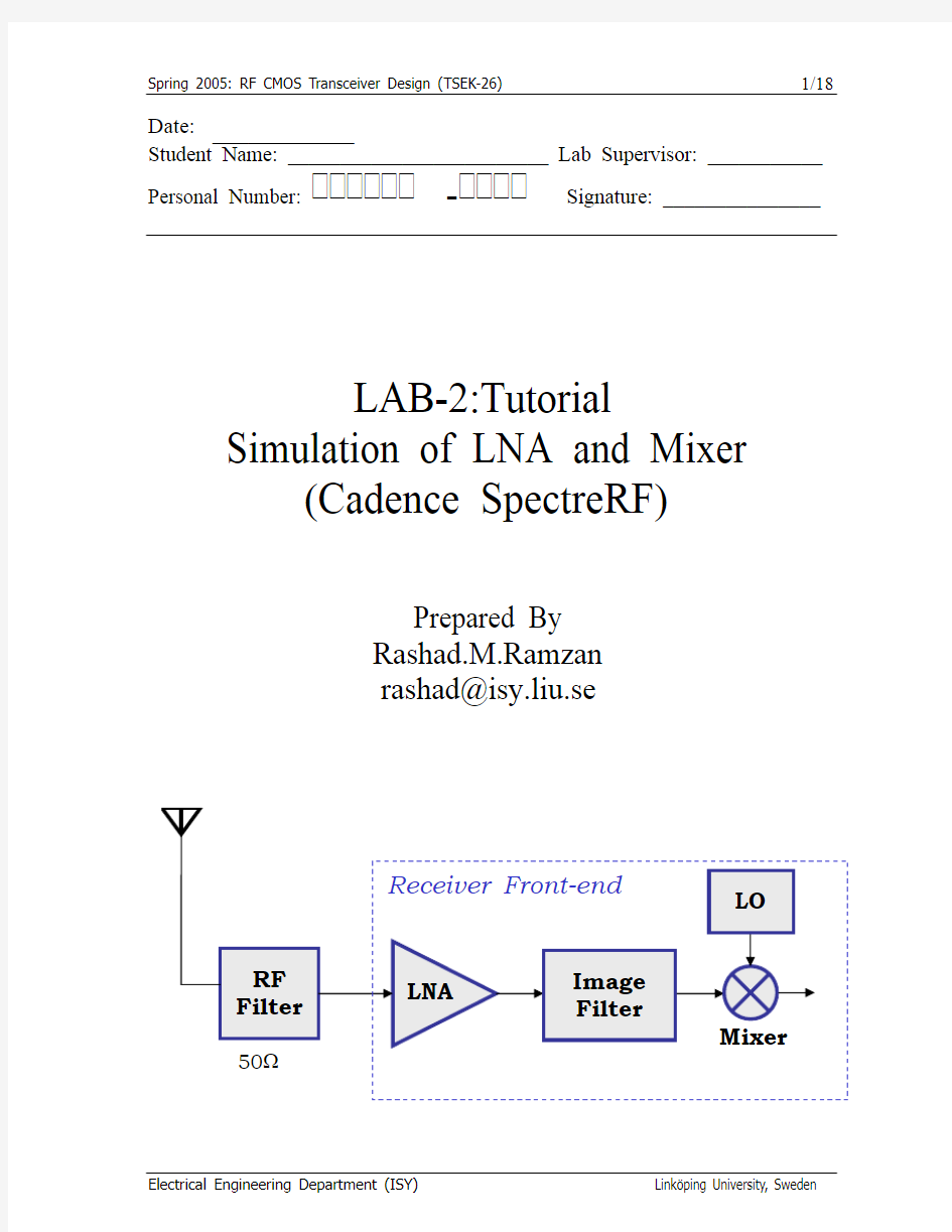
LAB-2:Tutorial Simulation of LNA and Mixer (Cadence SpectreRF)
Prepared By Rashad.M.Ramzan rashad@isy.liu.se
Receiver Front-end
LO
RF Filter
50?
LNA
Image Filter Mixer
Electrical Engineering Department (ISY)
Link?ping University, Sweden
Spring 2005: RF CMOS Transceiver Design (TSEK-26)
2/18
Introduction:
This Lab exercise consists of two parts: Part-I: LNA (Low Noise Amplifier Design) Simulation using SpectreRF. Part-II: (Optional) Mixer Simulation using SpectreRF. This Tutorial LAB describes how to use SpectreRF in Analog Design Environment to measure parameters which are important in design verification of Low Noise Amplifiers (LNA) and Mixer.
Instructions
? ? ? The LAB manual and related Application Notes (LNA Design Using SpectreRF and Mixer Design Using SpectreRF) are available on (TSEK-26) web page. To answer the question in this manual, please refer to the Application Note: LNA Design Using SpectreRF.
Part-II of Lab is optional, you can complete in your own time, if there is any problem please send an email or show up in the office of the TA. _________________________________________________________________________
Part-1: Low Noise Amplifier (LNA)
The LNA Design is the same as in the last problem in the class tutorial on LNAs (You can compare the hand calculated and simulated results!!). The component values are very close to hand calculation. Only small changes have been done to enhance the gain and Noise Figure of single ended source degenerated LNA. To character the LNA following figure of merits are usually measured. 1. Power Consumption and Supply Voltage 2. Gain 3. Noise 4. Input and Output Impedance Matching 5. Reverse Isolation 6. Stability 7. Linearity We will use S-Parameters (SP), Periodic Steady State Analysis (PSS), Periodic AC (PAC) and Pnoise analysis available in SpectreRF simulator to simulate above parameter of LNA. Usually there is more than one method available to simulate the desired parameter; we will use the procedure recommended by cadence. 1. S-Parameter Analysis ? Small Signal Gain (S21, GA, GT, GP) ? Small Signal Stability (Kf and ? or Bif ) ? Small Signal Noise (SP and Pnoise) ? Input and Output Matching (S11, S22, Z11, Z22) 2. Large Signal Noise Simulation (PSS and Pnoise) 3. Gain Compression, 1dB Compression Point (Swept PSS) 4. Large Signal Voltage Gain and Harmonic Distortion (PSS) 5. IP3 Simulation (Swept PSS) 6. Conversion Gain and Power Supply Rejection Ratio (PSS and PXF)
Electrical Engineering Department (ISY)
Link?ping University, Sweden
Spring 2005: RF CMOS Transceiver Design (TSEK-26)
3/18
1. Back Ground Preparation (LNA)
Please read the Application Note “LNA Design Using Specter RF” and answer the following questions before you attend the LAB. ? Define Transducer Power Gain (GT), Operating Power Gain (GP) and Available Power Gain (GA) for a two port network?
?
How we can relate the S-Parameters to the gain, input impedance and output impedance of any two-port network?
?
Why is the reverse isolation gain important in the LNA design? Which S-parameter directly characterizes the reverse isolation gain?
?
What is stern stability factor? What is minimum condition of stability for LNA?
?
Define the Power Supply Rejection Ratio (PSRR)? Look at the circuit diagram of LNA, what is your guess about the PSRR of this LNA?
Electrical Engineering Department (ISY)
Link?ping University, Sweden
Spring 2005: RF CMOS Transceiver Design (TSEK-26)
4/18
2. LNA Simulation
2.1. Circuit Simulation Setup: ? We will be using AMS 0.35μm CMOS (c35b4) process for these LABs. ? Load the Cadence and technology file using ? module add cadence/4.4.6 ? module add ams/3.60 ? Start cadence by typing ams_cds –tech c35b4 –mode fb& ? Make a new library RF_LAB1 in Cadence Library Manager ? Create and draw the Schematics, LNA_testbench a as shown in Fig-1 and LNA as shown in Fig-2. The components values are listed below for your convenience. ? Input Port in Schematic LNA_testbench 50 Ohms in Resistance 1 in Port Number Sine in Source Type frf1 in Frequency name 1 field frf in Frequency 1 field prf in Amplitude1(dBm) field ? Output Port in Schematic LNA_testbench 500 Ohms in Resistance 2 in Port Number ? Component Values in Schematic LNA_testbench Vdd = 3.3V, C1, C2= 10nF, CL= 500fF ? Component Values in LNA Schematic M1, M2 = 200μm/0.35μm , Mbias = 60μm/0.35μm Ls = 700 pH, Lg = 12 nH, Ld = 6 nH, Rd = 700 ? C1, C2= 10nF, CL= 500fF
Fig. 1: Test Bench of LNA Electrical Engineering Department (ISY) Link?ping University, Sweden
Spring 2005: RF CMOS Transceiver Design (TSEK-26)
?
? ? ?
5/18 Variable values in affirma Design Variable window (variables Copy from Cellview) frf = 2.4 Ghz and prf = -20dBm Open the Schematic LNA_testbench and Select Tools Analog Enviornment In Simulation Environment Window (affirma window) choose Setup Environment In field Analysis Order fill the following: dc pss pac pnoise (Important, if this field is not set PXF, Pnoise and PAC analysis will not work properly)
Fig. 2: Circuit Diagram of Source Inductor Degenerated LNA
Electrical Engineering Department (ISY)
Link?ping University, Sweden
Spring 2005: RF CMOS Transceiver Design (TSEK-26)
6/18
2.2.
Small Signal Gain, NF, Impedance Matching and Stability ( S-Parameter ) ? In the affirma window, select analysis-choose, the analysis choose window shows up Select sp for Analysis In port field click on select and then activate the schematic (if not activated automatically), choose the input port first and then the output port. The names of two selected ports will appear in Ports field. Sweep Variable frequency Sweep Range (start--stop) 1G to 5G Sweep Type Automatic Do Noise Yes Select Input and output ports accordingly by clicking Select and then clicking at the appropriate Port in Schematic Make sure that Enabled Box is checked then click OK. ? In the affirma window click on Simulation Netlist and Run to start the simulation, make sure that simulation completes without errors. ? Now in the affirma window click on the Results Direct plot S-parameters ? The S-parameters results window appears. ? Impedance Matching In the S-parameters Results window… Select Function SP Plot Type Rectangular Modifier dB20 Click S11 {S12, S22 and S21} press the PLOT button. Change the waveform window setting to make the plot look like Fig-3.
Fig. 3: S-Parameters of LNA Electrical Engineering Department (ISY) Link?ping University, Sweden
Spring 2005: RF CMOS Transceiver Design (TSEK-26)
7/18
?
GT, GA and GP (Different Type of Gains) In the S-parameters Results window…. Select Function GT, GA and GP (one by one) Plot Type Rectangular and Modifier dB10 Press the PLOT button, the results are shown in Fig-4.
Fig. 4: GT, GA and GP
The power gain GP is closer to the transducer gain GT than the available gain GA which means the input matching network is properly designed. That is, S11 is close to zero. ? NF (Noise Figure) In the S-parameters Results window… Select Function NF (and NFmin) Plot Type Rectangular Modifier dB10 Press PLOT. The results are shown in Fig-5. Stability Factor Kf and Bif (?) In the S-parameters Results window… Select Function Kf and Bif (one at a time) Plot Type Rectangular Press the PLOT button. The results are shown in Fig-6.
?
The Stern stability factor K and ? can be plotted in two ways. The stability curves for K and ? as plotted with respect to frequency sweep as shown in Fig-6 or they can be plotted as load stability circle (LSB) and source stability circle (SSB).
Electrical Engineering Department (ISY) Link?ping University, Sweden
Spring 2005: RF CMOS Transceiver Design (TSEK-26)
8/18
Fig. 5: NF, NFmin using S-Parameters
Fig. 6: Kf and Delta of LNA
Note: You can also measure the Z-parameters like Z11 and Z22. This might help in the input and output impedance matching circuit design. S11 or input matching can be improved by changing the source degeneration inductor (Ls)
Electrical Engineering Department (ISY)
Link?ping University, Sweden
Spring 2005: RF CMOS Transceiver Design (TSEK-26)
9/18
2.3. NF by Large Signal Noise Simulation (PSS and Pnoise Analysis) Use the PSS and Pnoise analyses for large-signal and nonlinear noise analyses, where the circuits are linearized around the periodic steady-state operating point. (Use the Noise and SP analyses for small-signal and linear noise analyses, where the circuits are linearized around the DC operating point.) As the input power level increases, the circuit becomes nonlinear, the harmonics are generated and the noise spectrum is folded. Therefore, you should use the PSS and Pnoise analyses. When the input power level remains low, the NF calculated from the Pnoise, PSP, Noise, and SP analyses should all match. ? ? Change the Input Port Parameters in the Schematic 50 Ohms in Resistance, 1 in Port Number , DC in Source Type Verify the variable values in the affirma window frf = 2.4 Ghz prf = -20 (Its meaning less in this simulation) In the affirma window, select Analysis Choose The Choose Analysis window shows up Select pss for Analysis Uncheck the Auto Calculate Box Beat Frequency 2.4G Output Harmonics 20 Accuracy Default Moderate Make sure that Enabled Box is checked then click OK. Now at the top of choosing Analysis window Select pnoise for Analysis PSS Beat Frequency(Hz) = 2.4GHz appears automatically Sweep Type Absolute Frequency Sweep Range Start: 1G Stop: 5G Sweep Type Automatic Maximum Sidebands 20 In output Section ? Select Voltage ? Positive Output Node Select net RF_OUT from Schematic ? Negative Output Node Leave Empty , it means GND ? Input Sources Select PORT ? Input PORT Source Select PORT1 from Schematic ? Reference Side Band 0 Noise Type Sources Enable Box in the bottom should be checked. Click OK In the affirma window click on Simulation Netlist and Run to start the simulation, make sure that simulation completes without errors. Now in the affirma window click on the Results Direct plot PSS
Link?ping University, Sweden
? ?
?
? ?
Electrical Engineering Department (ISY)
Spring 2005: RF CMOS Transceiver Design (TSEK-26)
10/18
?
The PSS results window appears. Plot mode Append Analysis Type pnoise Function Noise Figure Add to Output Box Unchecked Click on PLOT Button , results are shown in Fig-7.
Fig. 7: NF, Input and Output Noise using Pnoise Analysis
?
?
?
The Pnoise analysis summery shows you the contributions of different noise sources in the total noise. This is very powerful feature to focus the effort to improve the noise performance of the device which contributes the maximum noise. Now to see noise contribution in the affirma window click on the Results Print PSS Noise Summary Type Spot Noise Frequency Spot 2.4G Weighting flat Click on ALL TYPES button so that all entries are highlighted Truncate None Leave all other field as it is and press APPLY The Noise Contribution of Different Sources appears in new window Fill up the Table below indicating the noise contribution of different components.
Comp %Contribution Comp %Contribution Comp %Contribution Port1 M1
Electrical Engineering Department (ISY)
Link?ping University, Sweden
Spring 2005: RF CMOS Transceiver Design (TSEK-26)
11/18
2.4.
Large Signal Voltage Gain and Harmonic Distortion (PSS) ? Change the Input Port Parameters in Schematic Window 50 Ohms in Resistance 1 in Port Number Sine in Source Type frf1 in Frequency name 1 field frf in Frequency 1 field prf in Amplitude1(dBm) field ? Verify the variable values in the affirma window frf = 2.4 Ghz prf = -20dBm ? In the affirma window, select Analysis Choose ? The Choose Analysis window shows up Select pss for Analysis In Fundamental Tones following line shold be visible 1 frf1 frf 2.4G Large PORT1 Check the Auto Calculate Box Beat Frequency 2.4G (Automatically appears) No of Harmonics 10 Accuracy Default Moderate Enable Box in the bottom should be checked. Click OK ? In the affirma window click on Simulation Netlist and Run to start the simulation, make sure that simulation completes without errors. ? In the affirma window, select Results Direct plot PSS the analysis choose window shows up Select Function as Voltage Gain Modifier dB20 Input Harmonics 2.4G Select Output and Input nets and then activate the schematic window and select RF_OUT and RF_IN nets respectively. At the top of PSS result window change the plot mode to append. Now Select Function as Voltage Sweep Spectrum Signal Level peak Modifier dB20 Select net and the point to RF_OUT net in schematic ? Modify the display window. The results are shown in Fig-8.
After the PSS analysis, we can observe the harmonic distortion of the LNA by plotting the spectrum of any node voltage. Harmonic distortion is characterized as the ratio of the power of the fundamental signal divided by the sum of the power at the harmonics.
Electrical Engineering Department (ISY)
Link?ping University, Sweden
Spring 2005: RF CMOS Transceiver Design (TSEK-26)
12/18
2.5.
1dB Compression Point(Swept PSS) ? Change/Check the Input Port Parameters in Schematic Window 50 Ohms in Resistance 1 in Port Number Sine in Source Type frf1 in Frequency name 1 field frf in Frequency 1 field prf in Amplitude1(dBm) field ? Verify the variable values in the affirma window frf = 2.4 Ghz prf = -20dBm ? In the affirma window, select Analysis Choose ? The Choose Analysis window shows up Select pss for Analysis In Fundamental Tones following line shold be visible 1 frf1 frf 2.4G Large PORT1 Uncheck the Auto Calculate Box Beat Frequency 200K No of Harmonics 12 Accuracy Default Moderate High light the Sweep Button Click Design Variable Button, small window appears, choose prf in it Sweep Range Choose the start : -40dBm and Stop: 0dBm Sweep Type Liner and No of Steps =12 Enable Box in the bottom should be checked. Click OK ? In the affirma window click on Simulation Netlist and Run to start the simulation, make sure that simulation completes without errors. ? In the affirma window, select Results Direct plot PSS the analysis choose window shows up Select Function Compression Point Select Port (Fixed R (Port)) Gain Compression 1dB Extrapolation Point -40dB Ist Order Harmonic 2.4G Activate the Schematic Window and click on Output PORT to view the results as shown in Fig-9.
A PSS analysis calculates the operating power gain. That is, the ratio of power delivered to the load divided by the power available from the source. This gain definition is the same as that for GP. Therefore, the gain from PSS should match GP when the input power level is low and nonlinearity is weak. In case of differential LNA the even mode disturbances will be suppressed.
Electrical Engineering Department (ISY) Link?ping University, Sweden
Spring 2005: RF CMOS Transceiver Design (TSEK-26)
13/18
Fig. 8: Voltage Gain and Harmonic Distortion
Fig. 9: 1dB Compression Point
Electrical Engineering Department (ISY)
Link?ping University, Sweden
Spring 2005: RF CMOS Transceiver Design (TSEK-26)
14/18
2.6. IIP3 (Swept PSS) Two-tone test is used to measure an IP3 curve where the two tones, ω1 and ω2. Since the first-order components grow linearly and third-order components grow cubically, they eventually intercept as the input power level increases as shown in Fig-10. The IP3 is defined as the cross point of the power for the 1st order tones, ω1 and ω2, and the power for the 3rd order tones, 2ω1 – ω2 and 2ω2 - ω1, on the load side. ? There are three ways to Simulate IIP3, Using Swept PSS, PSS and PAC and QPSS. We will use Swept PSS Analysis. ? Change the Input Port Parameters in Schematic Window 50 Ohms in Resistance 1 in Port Number Sine in Source Type frf1 in Frequency name 1 field frf in Frequency 1 field prf in Amplitude1(dBm) field Click on the Box Display Second Sinusoid frf2 in Frequency name2 field frf+40M in Frequency2 field prf in Amplitude2(dBm) field ? Verify the variable values in the affirma window frf = 2.4 Ghz prf = -20dBm ? In the affirma window, select Analysis Choose ? The Choose Analysis window shows up Select pss for Analysis In Fundamental Tones, the following lines should be visible 1 frf1 frf 2.4G Large PORT1 2 frf1 frf+40M 2.44G Large PORT1 Check the Auto Calculate Box Beat Frequency 40M (Automatically appears) No of Harmonics 65 Accuracy Default Moderate High light the Sweep Button Select Design Variable, small window appears, choose prf in it Sweep Range Choose the start : -30dBm and Stop: 0dBm Sweep Type Liner and No of Steps =12 Enable Box in the bottom should be checked. Click OK In the affirma window click on Simulation Netlist and Run to start the simulation, make sure that simulation completes without errors. In the affirma window, select Results Direct plot PSS the analysis choose window shows up High light the Replace in Plot Mode Select Function as Compression Point
Link?ping University, Sweden
? ?
Electrical Engineering Department (ISY)
Spring 2005: RF CMOS Transceiver Design (TSEK-26)
15/18
Analysis PSS Function IPN Curves Select Port (Fixed R (Port)) Highlight variable Sweep Prf Extrapolation Point -30dB Highlight Input Referred IP3 Order 3rd 1st Order Harmonic 2.4G 3rd Order Harmonic 2.48G Activate the Schematic Window and click on Output port to view the results as shown in Fig-10.
Fig. 10: Input Referred IIP3
Electrical Engineering Department (ISY)
Link?ping University, Sweden
Spring 2005: RF CMOS Transceiver Design (TSEK-26)
16/18
2.7. Conversion Gain and Power Supply Rejection Ratio (PSS and PXF) The PXF analysis provides frequency dependent transfer function from any specific source to the designated output (RF_OUT in this case). If the specific source is power supply node then we can measure the PSRR. ? Change the Input Port Parameters in Schematic 50 Ohms in Resistance 1 in Port Number DC in Source Type Variable values in affirma window frf = 2.4 Ghz prf = -20 In the affirma window, select Analysis Choose The Choose Analysis window shows up Select pss for Analysis Uncheck the Auto Calculate Box Beat Frequency 2.4G Output Harmonics 4 Accuracy Default Conservative Now at the top of choosing Analysis window Select pxf for Analysis PSS Beat Frequency(Hz) = 2.4GHz (appears automatically) Frequency Sweep Range Start: 1G Stop: 5G Sweep Type Linear and Step Size 40M Maximum Sidebands 0 In output Section ? Select Voltage ? Positive Output Node Select net RF_OUT from Schematic ? Negative Output Node Leave Empty , it means GND Click OK In the affirma window click on Simulation Netlist and Run to start the simulation, make sure that simulation completes without errors. Now in the affirma window click on the Results Direct plot PSS The PSS results window appears. Select Analysis Type pxf Sweep Spectrum Function Voltage Gain Modifier dB20 Activate the Schematic window, click on INPUT port, OUTPUT port and VDD symbols. The Plots window pops up with plot as shown in Fig-11. Please note that PSRR is extremely poor. Why?
Link?ping University, Sweden
?
? ?
?
? ? ?
Electrical Engineering Department (ISY)
Spring 2005: RF CMOS Transceiver Design (TSEK-26)
17/18
Fig. 11: Transfer Function and PSRR
Electrical Engineering Department (ISY)
Link?ping University, Sweden
Spring 2005: RF CMOS Transceiver Design (TSEK-26)
18/18
Part-2: Mixer Design
To character the Mixer following figure of merits are usually measured. 1. 2. 3. 4. 5. 6. 7. Power Consumption RF to IF and LO to IF Conversion Gain Noise and NF Input and Output Impedance LO to RF and LO to IF Isolation Stability Linearity
The Application Note “Mixer Design Using SpectreRF” describes the details of different analysis using single balanced mixer used to characterize the above mentioned parameters of a Mixer. This part of LAB is optional, you can complete in your own time and if you face any difficulty you are welcome to contact the TAs of this course. The analyses listed below are sufficient to characterize the mixer for above mentioned seven parameters: 1. LNA (Low Noise Amplifier) as follow 2. Conversion Gain ? Voltage Conversion Gain Versus LO Signal Power (Swept PSS with PAC) ? Voltage Conversion Gain Versus RF Frequency (PSS and Swept PAC) ? Voltage Conversion Gain Versus RF Frequency (PSS and Swept PXF) ? Power Conversion Gain Versus RF Frequency (QPSS) 3. Power Dissipation (QPSS) 4. S-Parameters (PSS and PSP) 5. Total Noise and NF, SSB and DSB Noise Figures (PSS and Pnoise) 6. Intermodulation Distortion and Intercept Points (Swept QPSS and QPAC) 7. Port-to-Port Isolation Among RF, IF and LO Ports (PSS and Swept PAC) 8. Mixer Performance with a Blocking Signal (QPSS, QPAC, and QPNoise)
Electrical Engineering Department (ISY)
Link?ping University, Sweden