gerberFAB

Brightness-T
GERBER to FABMaster FATF 转换指南(GC-Powerplace)
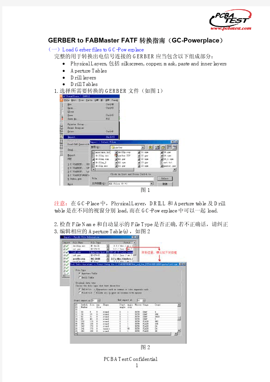
(一)Load Gerber files to GC-Powerplace (Shift+I) 完整的用于转换出电信号连接的 GERBER 应当包含以下组成部分: ? Physical Layers, 包括 silkscreen, copper, mask, paste and inner layers ? Aperture Tables ? Drill layers ? Drill Tables 1. 选择所需要转换的 GERBER 文件(如图 1)
20080924
图1 注意:在 GC-Place 中,Physical Layer,DRILL 和 Aperture table 及 Drill table 是在不同的视窗分别 load, 而在 GC-Powerplace 中可以一起 load. 2. 检查 File Name 和自动显示的 File Type 是否正确, 若不正确话,请纠正 3. 编辑相应的 Aperture Table(s) ,如图 2
图2 PCBATest Confidential 1
(1) 选择 Aperture Table 的起始行和结束行 (2) 选择列分割符,选择单位,选择 D-code, shape, x, y 所对应的列 (3) 按 Next 继续,直到按 OK 完成对 Aperture 的编辑 4. 仿照编辑 Aperture Table 的方法,编辑对应的 Drill Table(s)并确定好是 Plated 或 Un-plated (如图 3)
5. 根据 Customer 提供的 Readme 文件,确定 Physical Layer 和 Drill 导入时的 Format 例如: Drill (inch, leading, format 2.4), Gerber (mm, leading, Format 3.2) (图 4)
图4 6.根据 load 进来的每一层的具体内容,确定 Physical Layer Name, Type 和 Side(如图 5) PCBATest Confidential 2
图5 7. 按信号层的实际排列顺序排序,并根据 Readme 文件将具体的 drill 从哪 一层信号层穿到哪一层信号层(即通孔、埋孔还是盲孔)确定好(如图6) 双击任意 drill 层,在 GC-Explorer 对话框中单击“Edit Blind/Burier”按 钮,就会弹出如图 6 对话框。
图6 (二)Top Solder Paste 层转换出 Top Parts 层 如果没有 Top Solder Paste, 则可以从 Top Copper 层 Copy 所有元件的 pads 到 新的 Physical Layer,作为 Solder Paste 层使用。 1.将所有 Layers Hide, 只将 Top Solder Paste Layer 打开处于 Edit 状态,如 果有 Silkscreen Layer, 将对应的 Top Silkscreen Layer 打开处于 View 状态。 2.将 Trace 转换成 Pad (1) 将 Trace 和 Pad 用不同的颜色表示 (2) 选中所有需转换成 Pad 的 Trace(及 Pad) (3) 在 CAM 菜单中选择“Auto Convert Sketched Pads” (铜箔定位 /自动转 PAD )选项 (Ctrl+K)即可
PCBATest Confidential 3
Traces & Pads
Pad
3. 将 Pads 转换成 Parts (1) 选中 Solder Paste 层所有需转换成元件的 Pads (2) 选择 Parts 菜单中的“Automatic Centroid Extraction” (自动中心位置辨识)选项(@),GC- PowerPlace 会自动将 Pads 转换成 Parts,且会自动生成一层新的 Physical Layer (Name: ACE Top Parts, Type: Parts)。这层新的 Physical Layer 包含 两层 Data layer,即 “ACE Top Parts” ------ 所有自动转换出来的 Parts “ Footprint” ------------ 所有无法自动识别转换成 Parts 的 Pads
图7 注意:以前用 GC-Place,从 Solder Paste 层中转换出 Parts 以后, Solder Paste 层中相应的 Pads 就会消失,但用 GC-PowerPlace,会首先将 Solder Paste 层拷贝到 Footprint 层,然后从 Footprint 层转换出 Parts. 转换元件时注意元件的极性,若不确定时,可根据 AVL 中的 MPN 到网站上 Download data sheet. (3) 将自动转换错误的 Parts 打散,在 Footprint 层手工 Teach 元件,方法 如下:选中“ACE Top Parts”层自动转换出错的 Part,选择 Parts 菜单中 “Explode Parts”(Ctrl+Shift+E 零件或铜箔打散) 选项,即将转换 出错的元件 打散。在 Footprint 层 Unselect all, 选中需手工 Teach 成 Part 的 Pa ds, (Ctrl+Shift+P 零件教导) 选 项,在弹出的 选择 Parts 菜单中“Teach Part” 对话框中填好相应的信息,按 OK 即可。(如图 8) (三)Bottom side Solder Paste 层转换出 Bottom side Parts 层 若只有 Top Side, 则这一步的工作无需再做,直接跳到步骤(四)。 参照 Top Side 的方法,转换出 Bottom Side 的 Parts。
PCBATest Confidential 4
注意: 在 GC-Place 中,转换 Bottom Side 的元件时,需要首先把 Bottom Side 的 Solder Paste 层做一次镜像。而 GC-Powerplace 的人工智能会知道 Physical Layer 是 Bottom 时,所有元件必须是反转的(从 Top Side 透视 的看过去 Bottom Side),因此无需做镜像。
图8 (四)导入 Reference Designator Name 导入 Reference Name 有三种方法。方法 1:将 Parts 层与 Silkscreen 层相 匹配;方法 2:将 Parts 层与 CAD X-Y 相 Merge;方法 3:根据 Assembly Drawing 手工 Key in. 以下具体介绍方法 1,2。 1. 方法一:Parts Layer 与 Silkscreen 相匹配(以 Top Side 为例) 注意此法要求 Silkscreen 层 Location 的文字正好显示在元件的中心。若 是太偏的话,可能匹配不能完全成功。 (1) 将 Top Silkscreen 层和 Top Parts 层都打开处于 Edit 状态 (2) 确定文字层一个字母或数字的宽度和高度,方法如下: 将某个字母局部放大,十字光标移到它的左下脚,按 Z 键归零,再将 十字光标移至这个字母的右上脚,按空格键将光标定位在这一点。此 时在 Coordinates Summary 工具栏会显示这一个字母的宽度和高度(图 12)
PCBATest Confidential 5
图 12 (3) 选中 Parts 层和 Silkscreen 层,在 Parts 菜单中选中“Find Reference Designator(s) (I)”选项 (4) 在弹出的对话框中,按提示输入 Top Parts 及 Top Silkscreen 层的名字 (5) 输入一个字母或数字的宽度和高度 (如图 13) (6) 按 OK,会自动将 Silkscreen 层上 Reference Designator 的名字导入 Parts 层。 (7) 按“*”选中所有 Parts 层的元件,按“Q ”查看所有的 Reference Designator 名字是否都 Teach 到。若有遗漏,将遗漏的补全。(图 14)
图 13
图 14 2. 方法二:Merge CAD X-Y (1) Load CAD X-Y to GC-Powerplace PCBATest Confidential 6
在 File 菜单中选中“Load CAD Centroids…”选项,在弹出的对话框中输入 X-Y data 所在的路径(如图 9) 在紧接着弹出的对话框中按照提示填充读取 CAD X-Y 的规则,即起始 行、分隔符、单位及 ref.des, x, y, part#, angle, side 所对应的列序列号 (如图 10) 将 Load 进来的 CAD X-Y 层和 Parts 层打开处于 Edit 状态,两层对齐,在 Parts 菜单中选中 “Merger CAD Centroids”选项,在此后弹出的对话框中填入 CAD X-Y 所在物理层的名字及 Parts 层的名字(如图 11),按 OK 就会自 动将 Reference Designator Name 及 Part #导入。
图9
图 10
PCBATest Confidential 7
图 11 3.方法三:手工 Key In 元件的名字 (1) 将要 Key in Reference Name 的 Parts 层打开至 Edit 状态 (2) 选中所有要 Key in Reference Name 的 Parts,按 Q (Query) (3) Key in Reference Name 时,用 Ctrl 键加上、下键来帮助输入 (4) Key in Bottom Side Parts 时,可用右键选择 Bottom Side View, 这样的 话 Bottom 面的元件看上去就不是从 Top 面透视的了,便于 Key in. (五)将 BOM 中的 Part Number 导入到 GC-Powerplace 注意:能导入到 GC-PowerPlace 中的 BOM 一定要行列整齐的文本格式,不支 持 Excel 和 World 文档。 1.选中 Parts 层所有元件 2.在 Parts 下拉菜单中选中“Import Part Number(BOM)(Ctrl+Shift+B)”选项 3.在弹出的对话框中输入 BOM 文件的路径 (如图 15) 4.按下“BOM File Format Setting”按钮设置 BOM 导入时的格式(图 16) 在 Head Line 中输入起始行,在 Column 中输入起始的字节数,在 Width 中输入占用的字节数。 5.按 OK 键将 BOM 导入。 按 Q 键,查看所有元件的 Part Number 是否都 导入了,若有遗漏的请补全。
PCBATest Confidential 8
图 15
图 16 (六)Output X-Y Data for SMT 1. Output Top Side X-Y Data (1) 将 Parts 层打开处于 Edit 状态 (2) 设置好用户坐标零点 ( Zero User ) (3) 选中所有 Parts 层的元件 (4) 按 Q 键打开 Query 对话框 (5) 按“Save As”按钮,即可输出 Top X-Y Data for SMT。(图 17)
图 17 这里输出的 X-Y Data 是 Excel 格式的,后缀名为 CSV。而以前在 GCPlace 中输出的是后缀名为 LST 的文本格式。 2.Output Bottom Side X-Y Data 用以下方法输出的 Bottom 面元件的 X-Y Data 将不是从 Top Side 透视的 PCBATest Confidential 9
(1) (2) (3) (4)
(5)
(6) (7) (8)
新建一层 Unassigned Layer (系统设定新 Layer 为 U.1) 打开 Bottom Side 零件层,拷贝至 Unassigned Layer U.1 关闭所有层(Hide All Layers),只打开 U.1 为 Edit. 选中所有零件( Mark all parts of U.1) 用 Mirror X 在 X0 位置反转所有零件(Mirror X by X0 for All Selected Parts) 新建一层 Physical Layer (Include Data Layer) 将 U.1 拷贝至新的 Physical Layer. 参考 Top Side X-Y Data, 输出 Bottom Side 的 X-Y Data.
(七)Generate FATF file for Test (Include a Testability Analysis Report) 1.Extract Netlist (Ctrl+E) (1) 再次确定每一层上的 Drills 是 Plated 还是 Un-plated (2) 确定每一物理层的 Polarity,即是“+”、“-”还是“C”。例如: Solder Mask 层应是“-”,Copper 层是“+”,而内部层应根据具体情 况设定为“+”、“-”或“C”。 (3) 将所有的 Holes 和有用的 Physical Layers 打开处于 Edit 状态。注意没有 用的层可以将它拖到 Unassigned Layers 中(包括 Outline) (4) 在 Test 下拉菜单中选中“Extract Netlist”选项 (5) 在此后弹出的对话框中,根据提示输入对应的 Mask 和 Parts 层的层数 (或层名)(图 18) (6) 在 Test Point Strategy 中选择 Clamshell;Loop Test Points 选择 All (7) 按 OK 键开始 Extract Netlist. 这个过程比较长,请耐心等待。
图 18 2.Testability Report (1) 在 Test 下拉菜单中选择“Testability Report”选项 (2) 在弹出的对话框中根据提示选择 Top & Bottom Circuit Layer, Top & Bottom Parts Layer, Top & Bottom Mask Layer 及 Board Outline 对应的层 数(或层名);Output Format 选择 HTML;选择 Report 报告中需要包 含的信息 (图 19) (3) 按 OK 键会生成符合要求的 Testability Report 报告
PCBATest Confidential 10
图 19 3. Output FATF file (or Gencad file) (1) 在 File 下拉菜单中选择 Export-> FATF (Gencad) (图 20) (2) 在弹出的对话框中选择 Output 的路径,根据提示输入对应的层数(或 层名)(图 21) (3) 按 OK 键即可。
图 20
图 21 PCBATest Confidential 11
(八)如何修改 D-Code 大小 for Stencil 1. 选中需修改 D-Code 的焊盘。 2. 选择 EDIT 菜单中的 New Tools (Shift+N)选项 3. 在弹出的“Select an Aperture”对话框中按下 New Aper 按钮
4. 弹出“Add New Aperture”对话框,在 Aperture Typ 下拉框中选择新的 Dcode 的外形,在下面的输入框中输入对应的参数,按 OK 键 D-code 即修改成 功。
常用快捷键: 1. 2. 3. 4. S ---- Jump to the center of Pad, Part or Trace Space ---- Active the cursor Z ---- Set the relative coordinate to (0,0) Shift + N ---- New tool
PCBATest Confidential 12