DS1123LE-200+;DS1123LE-25+;DS1123LE-50+;DS1123LE-100+;中文规格书,Datasheet资料

General Description
The DS1123L is an 8-bit programmable timing element similar in function to the DS1023, but operating at 3.3V.Like the DS1023, the DS1123L can delay signals up to a full period or more when used as a delay line, and an on-chip reference delay can be used to offset the inher-ent “step-zero” delay. This allows the DS1123L to shift a clock signal over the full 0 to 360°phase range. In addition to functioning as a delay line, it can be config-ured as a free-running oscillator or an externally trig-gered monostable vibrator.
Applications
Telecommunications Digital Test Equipment Digital Video Projection
Signal Generators and Analyzers
Features
?Step Sizes of 0.25ns, 0.5ns, 1ns, 2ns
?On-Chip Reference Delay
?Configurable as a Delay Line, Monostable Vibrator, or Free-Running Oscillator ?Can Delay Signals by a Full Period or More ?Guaranteed Monotonicity
?Parallel and 3-Wire Serial Programming Interface ?Single 3.3V Power Supply ?16-pin TSSOP
DS1123L
3.3V , 8-Bit, Programmable Timing Element
_____________________________________________Maxim Integrated Products 1
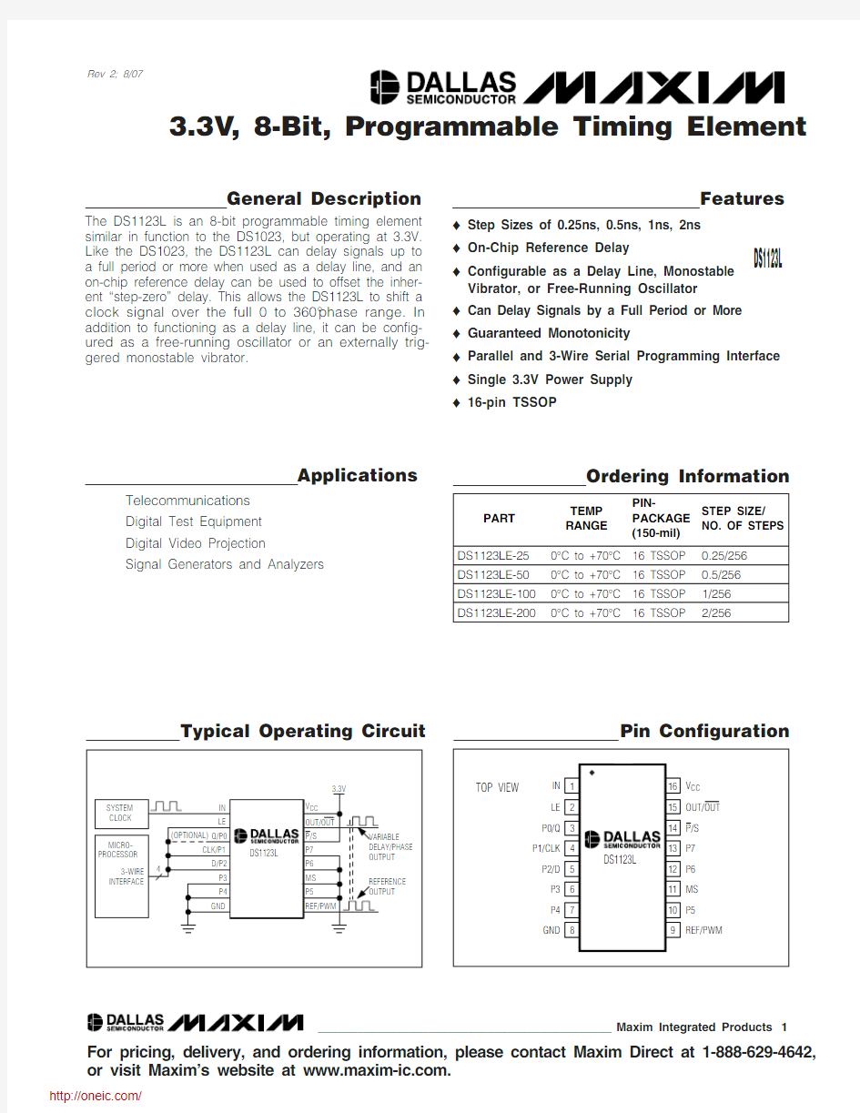
Pin Configuration
Typical Operating Circuit
Ordering Information
Rev 2; 8/07
For pricing, delivery, and ordering information, please contact Maxim Direct at 1-888-629-4642,or visit Maxim’s website at https://www.sodocs.net/doc/6112838563.html,.
D S 1123L
3.3V , 8-Bit, Programmable Timing Element 2______________________________________________________________________
ABSOLUTE MAXIMUM RATINGS
RECOMMENDED DC OPERATING CONDITIONS
(T A = 0°C to +70°C)
Stresses beyond those listed under “Absolute Maximum Ratings” may cause permanent damage to the device. These are stress ratings only, and functional operation of the device at these or any other conditions beyond those indicated in the operational sections of the specifications is not implied. Exposure to absolute maximum rating conditions for extended periods may affect device reliability.
Voltage Range on V CC Pin Relative to Ground.....-0.5V to +6.0V *Voltage Range on IN, LE, Q/P0, CLK/P1, D/P2, P3, P4, P5, MS,P6, P7, and P /S Relative to Ground..........-0.5V to V CC + 0.5V Operating Temperature Range...............................0°C to +70°C Storage Temperature Range.............................-55°C to +125°C
Short-Circuit Output Current.....................................50mA for 1s Soldering Temperature.......................................See IPC/JEDEC
J-STD-020A Specification
*Not to exceed +6.0V
DC ELECTRICAL CHARACTERISTICS
(V CC = +3.0 to 3.6V, T A = 0°C to +70°C.)
DS1123L
3.3V , 8-Bit, Programmable Timing Element
_____________________________________________________________________3
AC ELECTRICAL CHARACTERISTICS (ALL SPEED OPTIONS)
(V
= +3.0V to 3.6V, T = 0°C to +70°C.)
D S 1123L
3.3V , 8-Bit, Programmable Timing Element 4______________________________________________________________________
AC ELECTRICAL CHARACTERISTICS (DS1123L-25)
DS1123L
3.3V , 8-Bit, Programmable Timing Element
_____________________________________________________________________5
AC ELECTRICAL CHARACTERISTICS (DS1123L-50)
D S 1123L
3.3V , 8-Bit, Programmable Timing Element 6______________________________________________________________________
AC ELECTRICAL CHARACTERISTICS (DS1123L-100)
Note 2:If IN is high during power-up, the output remains low until IN is toggled low and back high again.
Note 3:The reference delay is closely matched to the step-zero delay to allow relative timings down to zero or less.Note 4:Measured from rising edge of the input to the rising edge of the output (t DR ).Note 5:Delay from input to output with a programmed delay value of zero.
Note 6:This is the relative delay between REF and OUT. The device is designed such that when programmed to zero delay the OUT output always appears before the REF output. This parameter is numerically equal to t D0 - t REF (see Figure 8).Note 7:From rising edge to rising edge.
Note 8:This is the actual measured delay from IN to OUT. This parameter exhibits greater temperature variation than the relative delay parameter.
Note 9:
This is the actual measured delay with respect to the REF output. This parameter more closely reflects the programmed delay value than the absolute delay parameter (see Figure 8). Typical delay shift due to aging is within ±0.85%. Aging stressing includes level 1 moisture reflow preconditioning (24hr +125°C bake, 168hr +85°C/85%RH moisture soak, and three solder reflow passes +260°C +0°C/-5°C peak) followed by 1000hr (max) V CC biased +125°C OP/L, 1000hr unbi-ased +150°C bake, and 1000 temperature cycles at -55°C to +125°C.
DS1123L
3.3V , 8-Bit, Programmable Timing Element
_____________________________________________________________________7
AC ELECTRICAL CHARACTERISTICS (DS1123L-200)
Note 11:Change in delay value when the inverted output is selected instead of the normal, noninverting output.Note 12:In PWM mode, the delay between the rising edge of the input and the rising edge of the output.
Note 13:The minimum value for which the monostable-vibrator pulse width should be programmed. Narrower pulse widths can be programmed, but output levels may be impaired and ultimately no output pulse is produced.
Note 14:
This is the minimum allowable interval between transitions on the input to assure accurate device operation. This parame-ter may be violated, but timing accuracy may be impaired and ultimately very narrow pulse widths result in no output from the device.
Note 15:
This parameter applies to normal delay mode only. When a 50% duty cycle input clock is used this defines the highest usable clock frequency. When asymmetrical clock inputs are used, the maximum usable clock frequency must be
reduced to conform to the minimum input pulse-width requirement. In PWM mode, the minimum input period is equal to the step-zero delay and the programmed delay (t DO +t D ).
Note 16:
Faster rise and fall times give the greatest accuracy in measured delay. Slow edges (outside the specification maximum)can result in erratic operations.
D S 1123L
3.3V , 8-Bit, Programmable Timing Element 8
______________________________________________________________________
Detailed Description
The DS1123L is an 8-bit programmable delay line that can be adjusted between 256 different delay intervals.Because of the design (see Figure 1) of the DS1123L, it is possible to delay a signal by a whole period or more,which allows the phase of the signal to be adjusted up to a full 360°. Programming may be done using either an 8-bit parallel interface or a 3-wire serial interface. Using the 3-wire interface, it is possible to cascade multiple devices together for systems requiring multiple pro-grammable delays without using additional I/O resources. The DS1123L also features a reference delay that is approximately equal to the step-zero delay, which can be used to realize small relative delays.Additionally, the DS1123L can function as a monostable vibrator or an adjustable frequency oscillator.
Device Operation
This section details how to program the DS1123L using both the parallel and serial interfaces, using the refer-ence delay, and how to configure the chip to function as a monostable vibrator or adjustable frequency oscillator.
Using the Parallel Programming Interface
To enable the DS1123L’s parallel interface, P /S must be connected to ground. This allows the data on the paral-lel inputs (P0 to P7) to pass through the latch, which are transparent when latch enable (LE) is at a high input level. When LE is at a low level, the data is latched until LE is returned to a high state. If the parallel inputs are going to be used to hardwire a delay, LE must be connected to V CC to allow the setting to take
DS1123L
3.3V , 8-Bit, Programmable Timing Element
_____________________________________________________________________
9
effect on power-up. The most flexibility when using par-allel mode occurs when the delay is being controlled by a microprocessor.
There are two common parallel interface implementa-tions used to control the DS1123L using a microproces-sor (see Figure 2). LE can be used to latch the data from the microprocessor, which allows the data bus to be shared with other peripherals, or LE can be tied
high, which causes the DS1123L to adjust its delay immediately following a change to the parallel inputs.For each configuration, a settling time (t EDV or t PDV ) is required after an adjustment is made before the input signal is accurately delayed according to the new set-ting. Figures 3 and 4 show the timing required for these implementations.
Using the Serial Programming Interface
The 3-wire serial interface is enabled by connecting P /S to V CC . Serial mode operates similar to a shift register.When LE is set at a high logic level, it enables the reg-ister and CLK clocks the data, D, into the register one bit at a time starting with the most significant bit. After all 8 bits are shifted into the DS1123L, LE is pulled low to end the data transfer and activate the new value. A settling time (t EDV ) is required after LE is pulled low before the signal delay meets its specified accuracy. A timing diagram for the serial interface is shown in Figure 6. The 3-wire interface also has an output (Q)that can be used to cascade multiple 3-wire devices,and it can be used to read the current value of the devices on the bus.
Figure 4. Latched Parallel Timing Diagram
D S 1123L
3.3V , 8-Bit, Programmable Timing Element 10
_____________________________________________________________________
To read the current values stored by the 3-wire device(s), the latch must be enabled and the value of Q must be read and then written back to D before the register is clocked. This causes the current value of the register to be written back into the DS1123L as it is being read. This can be accomplished in a couple of different ways. If the microprocessor has an I/O pin that is high impedance when set as an input, a feedback resistor (generally between 1k Ωand 10k Ω) can be used to write the data on Q back to D as the value is read (see Figure 5a). If the microprocessor has an internal pullup on its I/O pins, or only offers separate input and output pins, the value in the register can still
be read. The circuit shown in Figure 5b allows the Q values to read by the microprocessor, which must write the Q value to D before it can clock the bus to read the next bit. If the Q values are read without writing them to D (with the pullup or otherwise), the read is destructive.A destructive read cycle likely results in an undesirable change in the delay setting.
Figure 5c shows how to cascade multiple DS1123L’s onto the same 3-wire bus. One important detail of writ-ing software for cascaded 3-wire devices is that all the devices on the bus must be written to or read from dur-ing each read or write cycle. Attempting to write to only the first device (U1) would cause the data stored in U1
Figure 5. Using the Serial Interface
分销商库存信息:
MAXIM
DS1123LE-200+DS1123LE-25+DS1123LE-50+ DS1123LE-100+