AD9608BCPZ-105;AD9608BCPZ-125;AD9608BCPZRL7-105;AD9608BCPZRL7-125;中文规格书,Datasheet资料

10-Bit, 125/105 MSPS, 1.8 V Dual
Analog-to-Digital Converter (ADC)
AD9608 Rev. 0
Information furnished by Analog Devices is believed to be accurate and reliable. However, no
responsibility is assumed by Analog Devices for its use, nor for any infringements of patents or other rights of third parties that may result from its use. Specifications subject to change without notice. No license is granted by implication or otherwise under any patent or patent rights of Analog Devices. T rademarks and registered trademarks are the property of their respective owners. One Technology Way, P.O. Box 9106, Norwood, M A 02062-9106, U.S.A. Tel: 781.329.4700 https://www.sodocs.net/doc/763050550.html, Fax: 781.461.3113 ?2011 Analog Devices, Inc. All rights reserved.
FEATURES
1.8 V analog supply operation
1.8 V CMOS or 1.8 V LVDS output
SNR = 61.7 dBFS at 70 MHz
SFDR = 85 dBc at 70 MHz
Low power: 71 mW/channel ADC core at 125 MSPS Differential analog input with 650 MHz bandwidth
IF sampling frequencies to 200 MHz
On-chip voltage reference and sample-and-hold circuit
2 V p-p differential analog input
DNL = ±0.13 LSB
Serial port control options
Offset binary, Gray code, or twos complement data format Optional clock duty cycle stabilizer
Integer 1-to-8 input clock divider
Data output multiplex option
Built-in selectable digital test pattern generation
Energy-saving power-down modes
Data clock out with programmable clock and data
alignment
APPLICATIONS
Communications
Diversity radio systems
I/Q demodulation systems
Broadband data applications
Battery-powered instruments
Handheld scope meters
Portable medical imaging
Ultrasound
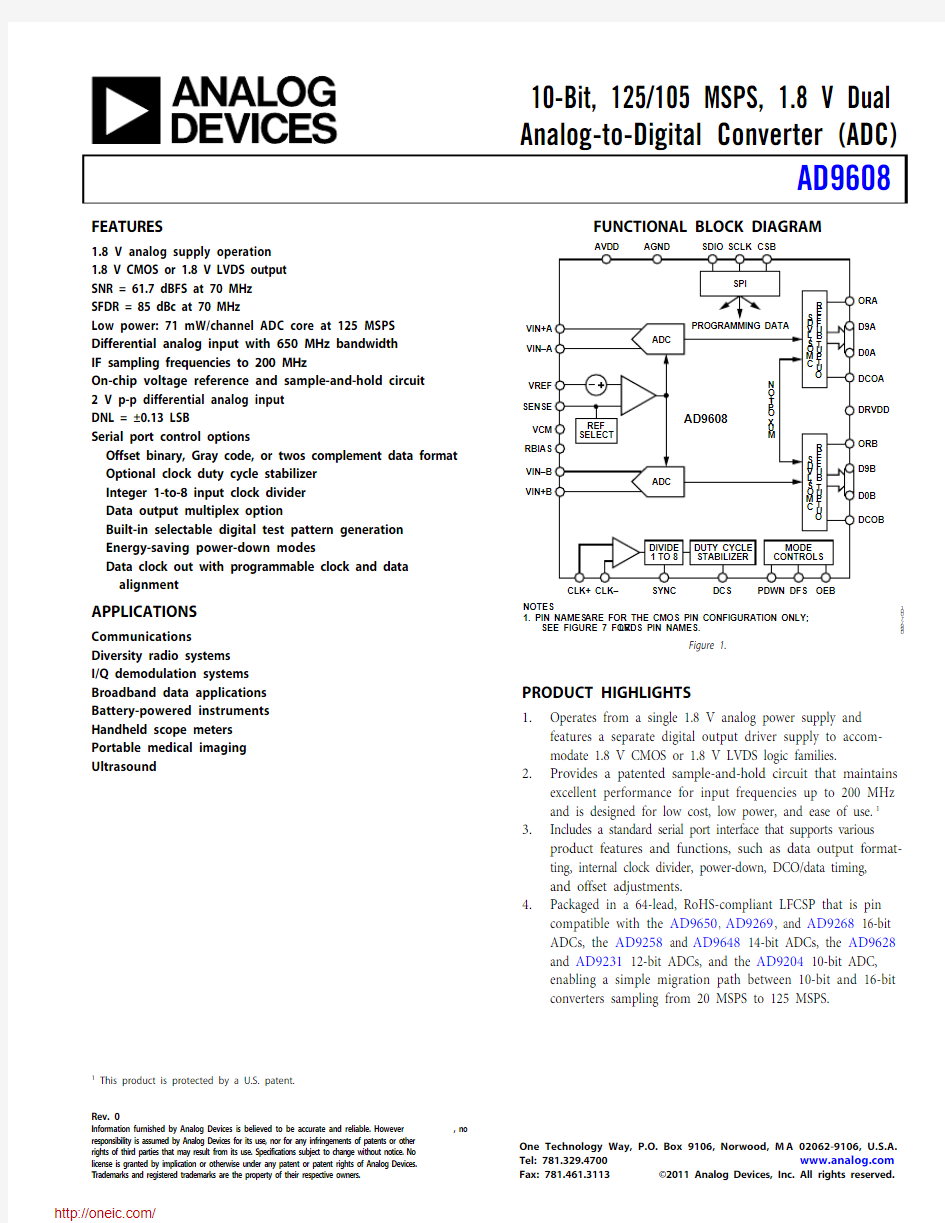
FUNCTIONAL BLOCK DIAGRAM
ORA
D0A
D9A
DCOA
DRVDD
ORB
D9B
D0B
DCOB
PDWN DFS
CLK+CLK–DCS
SYNC OEB
NOTES
1. PIN NAMES ARE FOR THE CMOS PIN CONFIGURATION ONLY;
SEE FIGURE 7 FOR LVDS PIN NAMES.0997
7
-
1
Figure 1.
PRODUCT HIGHLIGHTS
1.Operates from a single 1.8 V analog power supply and
features a separate digital output driver supply to accom-
modate 1.8 V CMOS or 1.8 V LVDS logic families.
2.Provides a patented sample-and-hold circuit that maintains
excellent performance for input frequencies up to 200 MHz and is designed for low cost, low power, and ease of use.1 3.Includes a standard serial port interface that supports various
product features and functions, such as data output format-ting, internal clock divider, power-down, DCO/data timing,
and offset adjustments.
4.Packaged in a 64-lead, RoHS-compliant LFCSP that is pin
compatible with the AD9650, AD9269, and AD9268 16-bit ADCs, the AD9258 and AD9648 14-bit ADCs, the AD9628 and AD9231 12-bit ADCs, and the AD9204 10-bit ADC,
enabling a simple migration path between 10-bit and 16-bit converters sampling from 20 MSPS to 125 MSPS.
1 This product is protected by a U.S. patent.
AD9608
Rev. 0 | Page 2 of 40
TABLE OF CONTENTS
Features..............................................................................................1 Applications.......................................................................................1 Functional Block Diagram..............................................................1 Product Highlights...........................................................................1 Revision History...............................................................................2 General Description.........................................................................3 Specifications.....................................................................................4 DC Specifications...........................................................................4 AC Specifications...........................................................................5 Digital Specifications...................................................................6 Switching Specifications................................................................7 Timing Specifications..................................................................8 Absolute Maximum Ratings..........................................................10 Thermal Characteristics............................................................10 ESD Caution................................................................................10 Pin Configurations and Function Descriptions.........................11 Typical Performance Characteristics...........................................17 AD9608-125................................................................................17 AD9608-105................................................................................20 Equivalent Circuits.........................................................................22 Theory of Operation......................................................................23 ADC Architecture......................................................................23 Analog Input Considerations....................................................23 Voltage Reference.......................................................................25 Clock Input Considerations......................................................26 Channel/Chip Synchronization................................................28 Power Dissipation and Standby Mode....................................28 Digital Outputs...........................................................................29 Timing.........................................................................................29 Built-In Self-Test (BIST) and Output Test..................................30 Built-In Self-Test (BIST)............................................................30 Output Test Modes.....................................................................30 Serial Port Interface (SPI)..............................................................31 Configuration Using the SPI.....................................................31 Hardware Interface.....................................................................32 Configuration Without the SPI................................................32 SPI Accessible Features..............................................................32 Memory Map..................................................................................33 Reading the Memory Map Register Table...............................33 Memory Map Register Table.....................................................34 Memory Map Register Descriptions........................................37 Applications Information..............................................................39 Design Guidelines......................................................................39 Outline Dimensions.......................................................................40 Ordering Guide.. (40)
REVISION HISTORY
7/11—Revision 0: Initial Version
AD9608
Rev. 0 | Page 3 of 40
GENERAL DESCRIPTION
The AD9608 is a monolithic, dual-channel, 1.8 V supply, 10-bit, 105 MSPS/125 MSPS analog-to-digital converter (ADC) that features a high performance sample-and-hold circuit and an on-chip voltage reference.
The product uses multistage differential pipeline architecture with output error correction logic to provide 10-bit accuracy at 125 MSPS data rates and to guarantee no missing codes over the full operating temperature range.
The ADC contains several features designed to maximize flexibility and minimize system cost, such as programmable clock and data alignment and programmable digital test pattern generation. The available digital test patterns include built-in deterministic and pseudorandom patterns, along with custom user-defined test patterns entered via the serial port interface (SPI).
A differential clock input controls all internal conversion cycles. An optional duty cycle stabilizer (DCS) compensates for wide variations in the clock duty cycle while maintaining excellent overall ADC performance.
The digital output data is presented in offset binary, Gray code, or twos complement format. A data output clock (DCO) is provided for each ADC channel to ensure proper latch timing with receiving logic. Logic levels of 1.8 V CMOS and 1.8 V LVDS are supported. Output data can also be multiplexed onto a single output bus. The AD9608 is available in a 64-lead RoHS-compliant LFCSP and is specified over the industrial temperature range (?40°C to +85°C). This product is protected by a U.S. patent.
AD9608
Rev. 0 | Page 4 of 40
SPECIFICATIONS
DC SPECIFICATIONS
AVDD = 1.8 V , DRVDD = 1.8 V , maximum sample rate, VIN = ?1.0 dBFS differential input, 1.0 V internal reference, DCS enabled, unless otherwise noted. Table 1.
AD9608-105 AD9608-125 Parameter Temp M in Typ M ax M in Typ M ax Unit RESOLUTION Full 10 10 Bits ACCURACY No Missing Codes Full Guaranteed Guaranteed Offset Error Full ?1.0 ?0.3 +0.4 ?1.0 ?0.3 +0.4 % FSR Gain Error Full ?2.8 ±1.5 +9.0 ?2.8 ±1.5 +9.0 % FSR Differential Nonlinearity (DNL)1 Full ±0.35 ±0.35 LSB 25°C ±0.12 ±0.13 LSB
Integral Nonlinearity (INL)1
Full ±0.40 ±0.40 LSB 25°C ±0.14 ±0.14 LSB MATCHING CHARACTERISTIC Offset Error Full ±0.1 ±1.0 ±0.1 ±1.0 % FSR Gain Error Full ±0.5 ±6.5 ±0.5 ±6.5 % FSR TEMPERATURE DRIFT Offset Error Full ±2 ±2 ppm/°C Gain Error Full ±50 ±50 ppm/°C INTERNAL VOLTAGE REFERENCE Output Voltage (1 V Mode) Full 0.98 1.00 1.02 0.98 1.00 1.02 V Load Regulation Error at 1.0 mA Full 2 2 mV INPUT REFERRED NOISE VREF = 1.0 V 25°C 0.08 0.08 LSB rms ANALOG INPUT Input Span, VREF = 1.0 V Full 2 2 V p-p Input Capacitance 2 Full 5 5 pF Input Resistance (Differential) Full 7.5 7.5 kΩ Input Common-Mode Voltage Full 0.9 0.9 V Input Common-Mode Range Full 0.5 1.3 0.5 1.3 V POWER SUPPLIES Supply Voltage AVDD Full 1.7 1.8 1.9 1.7 1.8 1.9 V DRVDD Full 1.7 1.8 1.9 1.7 1.8 1.9 V Supply Current
I AVDD 1
Full 76.8 82.0 87.7 93.0 mA I DRVDD 1 (1.8 V CMOS)
Full 14.7 17.4 mA I DRVDD 1 (1.8 V LVDS)
Full 48.5 49.7 mA POWER CONSUMPTION DC Input Full 125 141 mW
Sine Wave Input 1 (DRVDD = 1.8 V CMOS Output Mode)
Full 165 174 189 199 mW Sine Wave Input 1 (DRVDD = 1.8 V LVDS Output Mode)
Full 226 247 mW Standby Power 3 Full 108 120 mW Power-Down Power Full 2.0 2.0 mW
1 Measured with a low input frequency, full-scale sine wave, with approximately 5 pF loading on each output bit. 2
Input capacitance refers to the effective capacitance between one differential input pin and AGND. 3
Standby power is measured with a dc input and with the CLK± pins active (1.8 V CMOS mode).
AD9608
Rev. 0 | Page 5 of 40
AC SPECIFICATIONS
AVDD = 1.8 V , DRVDD = 1.8 V , maximum sample rate, VIN = ?1.0 dBFS differential input, 1.0 V internal reference, DCS enabled, unless otherwise noted. Table 2.
AD9608-105 AD9608-125 Parameter 1 Temp M in Typ M ax M in Typ M ax Unit SIGNAL-TO-NOISE-RATIO (SNR) f IN = 9.7 MHz 25°C 61.7 61.7 dBFS f IN = 30.5 MHz 25°C 61.7 61.7 dBFS f IN = 70 MHz 25°C 61.7 61.7 dBFS Full 61.3 61.3 dBFS
f IN = 100 MHz
25°C 61.6 61.6 dBFS f IN = 200 MHz 25°C 61.4 61.4 dBFS
SIGNAL-TO-NOISE AND DISTORTION (SINAD)
f IN = 9.7 MHz 25°C 61.6 61.6 dBFS f IN = 30.5 MHz 25°C 61.6 61.6 dBFS f IN = 70 MHz 25°C 61.6 61.6 dBFS Full 61.1 61.1 dBFS f IN = 100 MHz 25°C 61.5 61.5 dBFS
f IN = 200 MHz 25°C 61.3 61.3 dBFS
EFFECTIVE NUMBER OF BITS (ENOB)
f IN = 9.7 MHz 25°C 9.9 9.9 Bits f IN = 30.5 MHz 25°C 9.9 9.9 Bits f IN = 70 MHz 25°C 9.9 9.9 Bits f IN = 100 MHz 25°C 9.9 9.9 Bits f IN = 200 MHz 25°C 9.9 9.9 Bits WORST SECOND OR T H IRD H ARMONIC f IN = 9.7 MHz 25°C ?90 ?90 dBc f IN = 30.5 MHz 25°C ?89 ?89 dBc f IN = 70 MHz 25°C ?89 ?89 dBc Full ?75 ?75 dBc f IN = 100 MHz 25°C ?89 ?89 dBc f IN = 200 MHz 25°C ?84 ?84 dBc SPURIOUS-FREE DYNAMIC RANGE (SFDR) f IN = 9.7 MHz 25°C 85 85 dBc f IN = 30.5 MHz 25°C 85 85 dBc f IN = 70 MHz 25°C 85 85 dBc Full 75 75 dBc f IN = 100 MHz 25°C 85 85 dBc f IN = 200 MHz 25°C 84 84 dBc WORST OTHER (HARMONIC OR SPUR)
f IN = 9.7 MHz 25°C ?85 ?85 dBc f IN = 30.5 MHz 25°C ?85 ?85 dBc f IN = 70 MHz 25°C ?85 ?85 dBc
Full ?75 ?75
dBc f IN = 100 MHz 25°C ?85 ?85 dBc f IN = 200 MHz 25°C ?85 ?85 dBc
TWO-TONE SFDR
f IN = 29 MHz (?7 dBFS ), 32 MHz (?7 dBFS ) 25°C 82 82 dBc CROSSTALK 2
Full ?95 ?95 dB ANALOG INPUT BANDWIDTH
25°C 650 650 MHz
1 See the AN-835 Application Note, Understanding High Speed ADC Testing and Evaluation , for a complete set of definitions.
2
Crosstalk is measured at 100 MHz with ?1.0 dBFS on one channel and no input on the alternate channel.
AD9608
Rev. 0 | Page 6 of 40
DIGITAL SPECIFICATIONS
AVDD = 1.8 V , DRVDD = 1.8 V , maximum sample rate, VIN = ?1.0 dBFS differential input, 1.0 V internal reference, and DCS enabled, unless otherwise noted. Table 3.
Parameter Temp M in Typ M ax Unit DIFFERENTIAL CLOCK INPUTS (CLK+, CLK?) Logic Compliance CMOS/LVDS/LVPECL Internal Common-Mode Bias Full 0.9 V Differential Input Voltage Full 0.3 3.6 V p-p Input Voltage Range Full AGND ? 0.3 AVDD + 0.2 V Input Common-Mode Range Full 0.9 1.4 V High Level Input Current Full ?10 +10 μA Low Level Input Current Full ?10 +10 μA Input Capacitance Full 4 pF Input Resistance Full 8 10 12 kΩ LOGIC INPUT (CSB)1 High Level Input Voltage Full 1.22 DRVDD + 0.2 V Low Level Input Voltage Full 0 0.6 V High Level Input Current Full ?10 +10 μA Low Level Input Current Full 40 132 μA Input Resistance Full 26 kΩ Input Capacitance Full 2 pF
LOGIC INPUT (SCLK/DFS/SYNC)2
High Level Input Voltage Full 1.22 DRVDD + 0.2 V Low Level Input Voltage Full 0 0.6 V High Level Input Current (VIN = 1.8 V) Full ?92 ?135 μA Low Level Input Current Full ?10 +10 μA Input Resistance Full 26 kΩ Input Capacitance Full 2 pF
LOGIC INPUT/OUTPUT (SDIO/DCS)1
High Level Input Voltage Full 1.22 DRVDD + 0.2 V Low Level Input Voltage Full 0 0.6 V High Level Input Current Full ?10 +10 μA Low Level Input Current Full 38 128 μA Input Resistance Full 26 kΩ Input Capacitance Full 5 pF
LOGIC INPUTS (OEB, PDWN)2
High Level Input Voltage Full 1.22 DRVDD + 0.2 V Low Level Input Voltage Full 0 0.6 V High Level Input Current (VIN = 1.8 V) Full ?90 ?134 μA Low Level Input Current Full ?10 +10 μA Input Resistance Full 26 kΩ Input Capacitance Full 5 pF DIGITAL OUTPUTS CMOS Mode—DRVDD = 1.8 V High Level Output Voltage I OH = 50 μA Full 1.79 V I OH = 0.5 mA Full 1.75 V Low Level Output Voltage I OL = 1.6 mA Full 0.2 V I OL = 50 μA Full 0.05 V
AD9608
Rev. 0 | Page 7 of 40
Parameter Temp M in Typ M ax Unit LVDS Mode—DRVDD = 1.8 V Differential Output Voltage (V OD ), ANSI Mode Full 290 345 400 mV Output Offset Voltage (V OS ), ANSI Mode Full 1.15 1.25 1.35 V Differential Output Voltage (V OD ), Reduced Swing Mode Full 160 200 230 mV Output Offset Voltage (V OS ), Reduced Swing Mode Full 1.15 1.25 1.35 V
1 Pull up. 2
Pull down.
SWITCHING SPECIFICATIONS
AVDD = 1.8 V , DRVDD = 1.8 V , maximum sample rate, VIN = ?1.0 dBFS differential input, 1.0 V internal reference, and DCS enabled, unless otherwise noted. Table 4.
AD9608-105 AD9608-125 Parameter Temp M in Typ M ax M in Typ M ax Unit CLOCK INPUT PARAMETERS Input Clock Rate Full 1000 1000 MHz
Conversion Rate 1
DCS Enabled Full 20 105 20 125 MSPS DCS Disabled Full 10 105 10 125 MSPS CLK Period—Divide-by-1 Mode (t CLK ) Full 9.52 8 ns CLK Pulse Width High (t CH ) Full 4.76 4 ns Aperture Delay (t A ) Full 1.0 1.0 ns Aperture Uncertainty (Jitter, t J ) Full 0.07 0.07 ps rms DATA OUTPUT PARAMETERS CMOS Mode CMOS Mode (DRVDD = 1.8 V) Data Propagation Delay (t PD ) Full 1.8 2.9 4.4 1.8 2.9 4.4 ns DCO Propagation Delay (t DCO )2 Full 2.0 3.1 4.4 2.0 3.1 4.4 ns
DCO to Data Skew (t SKEW ) Full ?1.2 ?0.1 +1.0 ?1.2 ?0.1 +1.0 ns
LVDS Mode (DRVDD = 1.8 V)
Data Propagation Delay (t PD ) Full 2.4 2.4 ns
DCO Propagation Delay (t DCO )2 Full
4.4 4.4 ns DCO to Data Skew (t SKEW ) Full ?0.1 +0.2 +0.5 ?0.1 +0.2 +0.5 ns CMOS Mode Pipeline Delay (Latency) Full 16 16 Cycles
LVDS Mode Pipeline Delay (Latency)
Channel A/Channel B
Full 16/16.5 16/16.5 Cycles Wake-Up Time (Power-Down)3 Full 350 350 μs Wake-Up Time (Standby) Full 250 250 ns Out-of-Range Recovery Time Full 2 2 Cycles
1 Conversion rate is the clock rate after the divider.
2
Additional DCO delay can be added by writing to Bits[2:0] in SPI Register 0x17 (see Ta ). ble 183
Wake-up time is defined as the time required to return to normal operation from power-down mode.
AD9608
Rev. 0 | Page 8 of 40
TIMING SPECIFICATIONS
Table 5.
Parameter
Descriptions Limit SYNC TIMING REQUIREMENTS
t SSYNC SYNC to rising edge of CLK+ setup time 0.24 ns typ t HSYNC
SYNC to rising edge of CLK+ hold time 0.40 ns typ SPI TIMING REQUIREMENTS
t DS Setup time between the data and the rising edge of SCLK 2 ns min t DH Hold time between the data and the rising edge of SCLK 40 ns min t CLK Period of the SCLK
2 ns min t S Setup time between CSB and SCLK 2 ns min t H Hold time between CSB and SCLK 10 ns min t HIGH SCLK pulse width high 10 ns min t LOW SCLK pulse width low
10 ns min t EN_SDIO Time required for the SDIO pin to switch from an input to an output relative to the SCLK falling edge
10 ns min t DIS_SDIO
Time required for the SDIO pin to switch from an output to an input relative to the SCLK rising edge
2 ns min
Timing Diagrams
VIN
CLK+CLK–
CH A/CH B DATA DCOA/DCOB
09977-002
Figure 2. CMOS Default Output Mode Data Output Timing
VIN
CLK+CLK–
CH A DATA
DCOA/DCOB
CH B DATA
Figure 3. CMOS Interleaved Output Mode Data Output Timing
Rev. 0 | Page 9 of 40
Figure 4. LVDS Modes for Data Output Timing
SYNC
09977-005
Figure 5. SYNC Input Timing Requirements
AD9608
Rev. 0 | Page 10 of 40
ABSOLUTE MAXIMUM RATINGS
Table 6.
Parameter Rating
Electrical 1
AVDD to AGND ?0.3 V to +2.0 V
DRVDD to AGND ?0.3 V to +2.0 V
VIN+A/VIN+B, VIN?A/VIN?B to AGND ?0.3 V to AVDD + 0.2 V
CLK+, CLK? to AGND ?0.3 V to AVDD + 0.2 V
SYNC to AGND ?0.3 V to AVDD + 0.2 V
VCM to AGND ?0.3 V to AVDD + 0.2 V
RBIAS to AGND ?0.3 V to AVDD + 0.2 V
CSB to AGND ?0.3 V to DRVDD + 0.2 V
SCLK/DFS to AGND ?0.3 V to DRVDD + 0.2 V SDIO/DCS to AGND ?0.3 V to DRVDD + 0.2 V OEB ?0.3 V to DRVDD + 0.2 V PDWN ?0.3 V to DRVDD + 0.2 V
D0A, D0B through D9A, D9B to AGND ?0.3 V to DRVDD + 0.2 V DCOA , DCOB to AGND ?0.3 V to DRVDD + 0.2 V
Environmental
Operating Temperature Range
(Ambient) ?40°C to +85°C Maximum Junction Temperature Under Bias 150°C Storage Temperature Range
(Ambient)
?65°C to +150°C THERMAL CHARACTERISTICS
The exposed paddle must be soldered to the ground plane for
the LFCSP package. Soldering the exposed paddle to the PCB
increases the reliability of the solder joints and maximizes the
thermal capability of the package.
Table 7. Thermal Resistance Package Type Airflow Velocity (m/sec) θJA 1, 2 θJC 1, 3 θJB 1, 4 ΨJT 1, 2 Unit
0 22.3 1.4 N/A 0.1 °C/W 1.0 19.5 N/A 11.8 0.2 °C/W
64-Lead
LFCSP 9 mm × 9 mm
(CP-64-4)
2.5 17.5 N/A N/A 0.2 °C/W 1
Per JEDEC 51-7, plus JEDEC 25-5 2S2P test board. 2
Per JEDEC JESD51-2 (still air) or JEDEC JESD51-6 (moving air). 3
Per MIL-Std 883, Method 1012.1.
4
Per JEDEC JESD51-8 (still air).
Typical θJA is specified for a 4-layer PCB with a solid ground plane. As shown Table 7, airflow improves heat dissipation, which reduces θJA . In addition, metal in direct contact with the
package leads from metal traces, through holes, ground, and
power planes reduces θJA .
ESD CAUTION
1
The inputs and outputs are rated to the supply voltage (AVDD or DRVDD) +
0.2 V but should not exceed 2.1 V.
Stresses above those listed under Absolute Maximum Ratings may cause permanent damage to the device. This is a stress rating only; functional operation of the device at these or any other conditions above those indicated in the operational
section of this specification is not implied. Exposure to absolute maximum rating conditions for extended periods may affect device reliability.
分销商库存信息:
ANALOG-DEVICES
AD9608BCPZ-105AD9608BCPZ-125AD9608BCPZRL7-105 AD9608BCPZRL7-125AD9608-125EBZ