ISL97801ARZ-TK;ISL97801ARZ-T;ISL97801ARZ;ISL97801BOOSTEVALZ;中文规格书,Datasheet资料

?
FN6428.1
ISL97801
High Power LED Driver
The ISL97801 is a high-power LED backlight driver with an integrated 36V FET designed to drive up to 8 high-power LEDs in series. The PWM converter runs from an internally generated 1MHz clock. With efficiencies over 90% the regulator provides tight control of LED current and may be configured in either boost or buck topologies, allowing from 3 to 8 series diodes to be driven from wide input voltages. LED light level may be controlled either by: 1.LED DC bias current set via the LEVEL pin, or 2.External low frequency PWM control via the ENABLE/PWM pin.
In both control modes optional over temperature thermal protection of the LED reduces the LED DC bias current above an adjustable set temperature, protecting the LED from thermal damage. An optional fault monitor drives an external FET between the input supply and inductor, providing short circuit current protection for the LED and inductor as well as load dump protection for automotive applications. For low cost applications the pass transistor may be omitted and the fault pin bypassed.
The ISL97801 is packaged in a 20 Ld 4mm x 4mm QFN package and is specified for operation over the -40°C to +105°C temperature range.
Features
?Drives 3-8 high-power LEDs in series, up to 32V ? 2.7V to 16V input voltage range ?Boost or Buck configurable switch ?3A integrated FET
?Automotive load dump protection ?Light output temperature compensation ?LED over-temperature protection ?LED disconnect
?PWM/analog light level control
?Small, 20 Ld 4mm x 4mm QFN package ?Pb-free plus anneal available (RoHS compliant)
Applications
?Display backlighting -Automotive -LCD monitor
-Notebook displays ?LED accent lighting ?Automotive lighting
Pinout
ISL97801(20 LD 4X4 QFN)TOP VIEW
Ordering Information
PART NUMBER (Note)PART
MARKING TAPE & REEL/QTY PACKAGE (Pb-free)
PKG. DWG. #
ISL97801ARZ
978 01ARZ
-20 Ld 4x4 QFN L20.4x4C
ISL97801ARZ-TK 978 01ARZ 13”/1,00020 Ld 4x4 QFN L20.4x4C ISL97801ARZ-T
978 01ARZ
13”/6,000
20 Ld 4x4 QFN L20.4x4C
NOTE:Intersil Pb-free plus anneal products employ special Pb-free material sets; molding compounds/die attach materials and 100% matte tin plate termination finish, which are RoHS compliant and compatible with both SnPb and Pb-free soldering operations. Intersil Pb-free products are MSL classified at Pb-free peak reflow temperatures that meet or exceed the Pb-free requirements of IPC/JEDEC J STD-020.
B U
C K /B O O S T L E V E T E M F I N
A U L T
N D
C
T M A B A T
Data Sheet
April 2, 2007
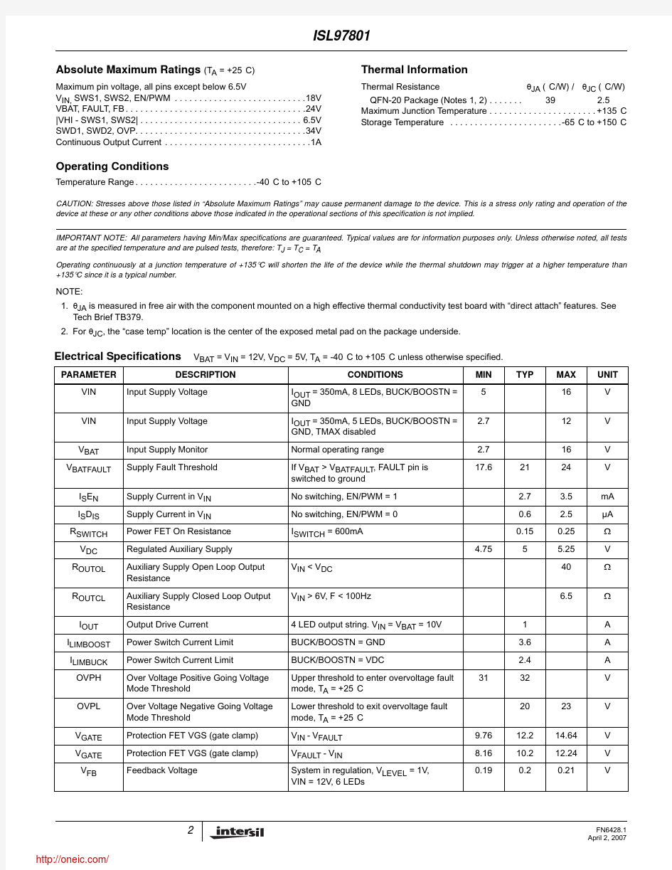
Absolute Maximum Ratings (T A = +25°C)Thermal Information
Maximum pin voltage, all pins except below 6.5V
V IN, SWS1, SWS2, EN/PWM . . . . . . . . . . . . . . . . . . . . . . . . . . .18V VBAT, FAULT, FB. . . . . . . . . . . . . . . . . . . . . . . . . . . . . . . . . . . . .24V |VHI - SWS1, SWS2|. . . . . . . . . . . . . . . . . . . . . . . . . . . . . . . . . 6.5V SWD1, SWD2, OVP. . . . . . . . . . . . . . . . . . . . . . . . . . . . . . . . . . .34V Continuous Output Current . . . . . . . . . . . . . . . . . . . . . . . . . . . . . .1A Operating Conditions
Temperature Range. . . . . . . . . . . . . . . . . . . . . . . . .-40°C to +105°C Thermal ResistanceθJA (°C/W) /θJC (°C/W) QFN-20 Package (Notes 1, 2) . . . . . . .39 2.5 Maximum Junction Temperature . . . . . . . . . . . . . . . . . . . . . .+135°C Storage Temperature . . . . . . . . . . . . . . . . . . . . . . .-65°C to +150°C
CAUTION: Stresses above those listed in “Absolute Maximum Ratings” may cause permanent damage to the device. This is a stress only rating and operation of the device at these or any other conditions above those indicated in the operational sections of this specification is not implied.
IMPORTANT NOTE:All parameters having Min/Max specifications are guaranteed. Typical values are for information purposes only. Unless otherwise noted, all tests are at the specified temperature and are pulsed tests, therefore: T J = T C = T A
Operating continuously at a junction temperature of +135°C will shorten the life of the device while the thermal shutdown may trigger at a higher temperature than +135°C since it is a typical number.
NOTE:
1.θJA is measured in free air with the component mounted on a high effective thermal conductivity test board with “direct attach” features. See
Tech Brief TB379.
2.For θJC, the “case temp” location is the center of the exposed metal pad on the package underside.
Electrical Specifications V BAT = V IN = 12V, V DC = 5V, T A = -40°C to +105°C unless otherwise specified.
PARAMETER DESCRIPTION CONDITIONS MIN TYP MAX UNIT VIN Input Supply Voltage I OUT = 350mA, 8 LEDs, BUCK/BOOSTN =
GND
516V
VIN Input Supply Voltage I OUT = 350mA, 5 LEDs, BUCK/BOOSTN =
GND, TMAX disabled
2.712V
V BAT Input Supply Monitor Normal operating range 2.716V V BATFAULT Supply Fault Threshold If V BAT > V BATFAULT, FAULT pin is
switched to ground
17.62124V
I S E N Supply Current in V IN No switching, EN/PWM = 1 2.7 3.5mA
I S D IS Supply Current in V IN No switching, EN/PWM = 00.6 2.5μA
R SWITCH Power FET On Resistance I SWITCH = 600mA0.150.25ΩV DC Regulated Auxiliary Supply 4.755 5.25V R OUTOL Auxiliary Supply Open Loop Output
Resistance
V IN < V DC40Ω
R OUTCL Auxiliary Supply Closed Loop Output
Resistance
V IN > 6V, F < 100Hz 6.5Ω
I OUT Output Drive Current 4 LED output string. V IN = V BAT = 10V1A
I LIMBOOST Power Switch Current Limit BUCK/BOOSTN = GND 3.6A
I LIMBUCK Power Switch Current Limit BUCK/BOOSTN = VDC 2.4A
OVPH Over Voltage Positive Going Voltage
Mode Threshold Upper threshold to enter overvoltage fault
mode, T A = +25°C
3132V
OVPL Over Voltage Negative Going Voltage
Mode Threshold Lower threshold to exit overvoltage fault
mode, T A = +25°C
2023V
V GATE Protection FET VGS (gate clamp)V IN -V FAULT9.7612.214.64V V GATE Protection FET VGS (gate clamp)V FAULT -V IN8.1610.212.24V V FB Feedback Voltage System in regulation, V LEVEL = 1V,
VIN = 12V, 6 LEDs
0.190.20.21V
V LEVEL Light Control Voltage Linear Input Range Mode = 1, analog control of LED current 0.253V FB UV FAULT Feedback Undervoltage Fault VLEVEL = 1V, EN/PWM = 3V 120160180mV FB OV FAULT
Feedback Overvoltage Fault VLEVEL = 1V, EN/PWM = 3V
220250280mV f SW Switching Frequency
850
10001150
kHz f DIMMING Maximum Recommended PWM Dimming Frequency Mode = 1, modulation signal applied to EN/PWM 10kHz t SWITCH Load Switch Transition Time C GATE = 2nF 100ns RLS DRIVERL Load Switch Driver Impedance Low EN/PWM = 03050ΩRLS DRIVERH
Load Switch Driver Impedance High EN/PWM = 3V
3050Ωt FAULT Fault Timer Period 40
5058ms t DELAY Start-up Delay
Timed LX switching delay 0.851
1.17
ms V FAULTPUMP Fault Pin Charge Pump V BAT = V IN = 3V 6
V V BOOST Boost Mode Threshold BUCK/BOOSTN = GND 0.4V DC
V V BUCK Buck Mode Threshold BUCK/BOOSTN = V DC 0.94V DC
V V MODEL Mode Low Threshold MODE = GND 1/3V DC
V V MODEH Mode High Threshold
MODE = V DC
2/3V DC
V en FAULT Input Level Applied to TMAX Pin to Enable Fault Protection
0.9V DC
V dis FAULT Input Level Applied to TMAX Pin to Disable Fault Protection
0.96V DC V en TEMP Input Level Applied to TEMP Pin to Enable Temperature Compensation 0.5
V dis TEMP Input Level Applied to TEMP Pin to Disable Temperature Compensation 0.08
V
T COMPP VFB Positive Temperature Compensation; VFB/VFBnom VTEMP/VDC = 0.80 1.26T COMPN VFB Negative Temperature Compensation; VFB/VFBnom VTEMP/VDC = 0.20
0.74T TRIP Internal Temperature Protection Threshold
135°C T HYS Internal Temperature Protection Hysteresis
25
°C VEN/PWM L EN/PWM Pin Input Low Threshold 1.2
V VEN/PWM H EN/PWM Pin Input High Threshold 2.5
V V DCUVLO V DC Under Voltage Lockout 2.6
V Rschottky
Internal Schottky Diode for Buck
15
23
Ω
Electrical Specifications
V BAT = V IN = 12V, V DC = 5V, T A = -40°C to +105°C unless otherwise specified. (Continued)
PARAMETER DESCRIPTION
CONDITIONS
MIN TYP
MAX UNIT TABLE 1.LIGHT OUTPUT CONTROL, V DC = 5.0V
MODE TEMP
OPERATING MODE
1 (VDC - 0.25) > V > 0.25V Standard Mode light level to PWM modulation of EN/PWM input; LED bias current determined by
LEVEL voltage, nominal 1V
Don’t Care
V < 0.25V Disable temperature compensation
V < (VDC - 0.25)
Fixed Bias Mode V FB level internally set to 0.4V, independent of V LEVEL
Typical Performance Curves
FIGURE 1.8 LEDs EFFICIENCY vs INPUT VOLTAGE vs
DIMMING FREQUENCY AND DUTY CYCLE FIGURE 2.5 LEDs EFFICIENCY vs INPUT VOLTAGE vs
DIMMING FREQUENCY AND DUTY CYCLE
FIGURE 3.3 LEDs EFFICIENCY vs INPUT VOLTAGE vs DIMMING FREQUENCY AND DUTY CYCLE
FIGURE 4.8 AND 5 LEDs EFFICIENCY vs PWM DUTY CYCLE
FIGURE 5.LEDs PWM DIMMING LINEARITY FIGURE 6.8 LEDs CURRENT ACCURACY vs INPUT VOLTAGE
6065707580
859095100
6
8
10
1214
16
18
V IN (V)
E F F I C I E N C Y (%)
8 LEDs
I LEDpeak = 380mA 10%@100Hz
10%@10kHz
99%@100Hz
99%@10kHz
50%@1kHz
50%@10kHz
50%@100Hz
10%@1kHz
99%@1kHz 6065707580859095100
4
6
8
1012
14
16
V IN (V)
E F F I C I E N C Y (%)
5 LEDs
I LEDpeak = 380mA
99% @ 10kHz
99% @ 100Hz
10% @ 10kHz
10% @ 100Hz 60657075808590
95100
4
8
10
V IN (V)
E F F I C I E N C Y (%)
3 LEDs I LEDpeak = 380mA 6
99%@100Hz
99%@10kHz
10%@10kHz
10%@100Hz 6065
707580859095
1000
20406080100
PWM DIMMING DUTY CYCLE (%)
E F F I C I E N C Y (%)
8 LEDs
5 LEDs
I LEDpeak = 380mA PWM = 10kHz 8 LEDs, V IN = 12V 5 LEDs, V IN = 9V
050100150200250300
350
4000
20
40
60
80
100
PWM DIMMING DUTY CYCLE (%)
I L E D (m A )
8 LEDs, V IN = 12V I LEDpeak = 380mA
5 LEDs @ 100Hz
5 LEDs, V IN = 9V 3 LEDs, V IN = 5V 3 LEDs @ 100Hz
8 LEDs @ 1kHz
5 LEDs @ 10kHz 8 LEDs @ 10kHz
-6-5
-4-3-2-101234
6
8
10
1214
16
18
V IN (V)
ΔI L E D (%)
8 LEDs
I LEDpeak = 380mA
10% @ 100Hz
99% @ 100Hz 99% @ 10kHz 10% @ 10kHz
FIGURE 7.5 LEDs CURRENT ACCURACY vs INPUT VOLTAGE FIGURE 8.3 LEDs CURRENT ACCURACY vs INPUT VOLTAGE
FIGURE 9.8 LEDs LINE REGULATION OF PWM DUTY
CYCLE OF 99%FIGURE 10.5 LEDs LINE REGULATION OF PWM DUTY
CYCLE OF 99%
FIGURE 11.3 LEDs LINE REGULATION OF PWM DUTY
CYCLE OF 99%FIGURE 12.8 LEDs LINE REGULATION OF PWM DUTY
CYCLE OF 10%
-10
-8-6-4-202468104
6
8
1012
14
16
V IN (V)
ΔI L E D (%)
5 LEDs
I LEDpeak = 380mA
10% @ 100Hz
10% @ 10kHz 99% @ 100Hz 99% @ 10kHz -4-2024681012141610
9
8
76
5
4
V IN (V)
ΔI L E D (%)
3 LEDs
I LEDpeak = 380mA
99% @ 100Hz
99% @ 10kHz
350
355360365370375380
385390395400
6
8
10
1214
16
18
V IN (V)
I L E D (m A )
8 LEDs I
LEDpeak = 380mA PWM @ 100Hz PWM @ 10kHz DUTY CYCLE = 99%PWM @ 1kHz
350
3553603653703753803853903954004054104154204
6
8
1012
14
16
I L E D (m A )
V IN (V)
5 LEDs
I LEDpeak = 380mA 99% @ 100Hz
DUTY CYCLE = 99%
99% @ 10kHz
360
365370375380385390
395
4004054104
5
6
78
9
10
I L E D (m A )
3 LEDs
I LEDpeak = 380mA PWM @ 100Hz DUTY CYCLE = 99%
PWM @ 10kHz
V IN (V)
3031
323334353637383940
6
8
10
12141618
I L E D (m A )
8 LEDs I
LEDpeak = 380mA DUTY CYCLE = 10%PWM @ 10kHz
V IN (V)
PWM @ 100Hz
PWM @ 1kHz
FIGURE 13.5 LEDs LINE REGULATION OF PWM DUTY
CYCLE OF 10%FIGURE 14.3 LEDs LINE REGULATION OF PWM DUTY
CYCLE OF 10%
FIGURE 15.LED CURRENT vs V LEVEL BIAS
FIGURE 16.QUIESCENT CURRENT (NON-SWITCHING)
FIGURE 17.START-UP WAVEFORMS FIGURE 18.START-UP WAVEFORMS ZOOM-IN
34
35363738394041
6
8
10
1214
16
18
I L E D (m A )
V IN (V)
10% @ 100Hz
10% @ 10kHz
5 LEDs
I LEDpeak = 380mA
DUTY CYCLE = 10%3233
343536373839404142
4
5
6
78
9
10
I L E D (m A )
V IN (V)
3 LEDs I
LEDpeak = 380mA DUTY CYCLE = 10%PWM @ 10kHz PWM @ 100Hz
050100150200250300350400
0.2
0.40.60.8
1.0
V LEVEL (V)
I L E D (m A )
RSET = 0.5Ω
DUTY CYCLE = 100%5 LED
3 LED
8 LED
0.0001
0.001
0.01
0.1
6
810
12141618
V IN (V)
I Q (m A )
EN/PWM = 0V LEVEL = 1V T A = +25°C
8 LEDs I LED = 350mA
8 LEDs I LED = 350mA
FIGURE 19.50% PWM DIMMING AT 100Hz FIGURE 20.50% PWM DIMMING AT 10kHz
FIGURE 21.10% PWM DIMMING AT 1kHz FIGURE 22.50% PWM DIMMING AT 1kHz ZOOM-IN
FIGURE 23.TRANSIENT RESPONSE OPERATES FROM
8 TO 7 LEDs
FIGURE 24.TRANSIENT RESPONSE OPERATES FROM
7 TO 8 LEDs
8 LEDs V IN = 16V PWM = 100Hz
8 LEDs V IN = 16V PWM = 10kHz
8 LEDs V IN = 12V PWM = 1kHz
PWM = 1kHz
DUTY CYCLE = 50%8 LEDs V IN = 16V TRANSIENT RESPONSE WHEN LOAD DYNAMICALLY
V IN = 12V I LED = 350mA
CHANGES FROM 8 LEDs TO 7 LEDs
8 LEDs V O
7 LEDs V O
TRANSIENT RESPONSE WHEN LOAD DYNAMICALLY V IN = 12V I LED = 350mA
CHANGES FROM 7LEDs TO 8LEDs 7 LEDs V O
8 LEDs V O
Typical Boost Mode Application Diagram
FIGURE 25.OVP AND RESET FIGURE 26.CURRENT LIMIT
FB = 0V
8LEDs V IN = 3.3V I LED = 380mA
VHI SWD1SWD2OVP
SWS1SWS2ENL GND
VIN FAULT VBAT
VDC
BUCK/BOOSTN TEMP TMAX
EN/PWM MODE LEVEL
V BAT
V DC
0.1μF
PWM
1V
FB FIGURE 27.TYPICAL BOOST MODE APPLICATION CIRCUIT
TEMP SENSOR
Pin Descriptions
PIN NAME DESCRIPTION
1VDC Internally regulated 5V supply, tracks V IN for input voltages less than 5V. LDO output can also be biased with external supply if VIN is <5.5V. A minimum of 3.3μF decoupling capacitor is needed in this pin.
2VHI Power FET gate drive supply. Can be biased with external supply if Vin is <5.5V
3OVP Overvoltage monitor input; tie to VOUT for normal operation
4SWD1NMOS power FET drain
5SWD2NMOS power FET drain
6BUCK/BOOSTN Tie to GND for BOOST operation and to VDC for Buck operation
7LEVEL Sets LED bias current level; VFB(nominal) = VLEVEL/5
8TEMP Temperature reference, tie to GND to disable temperature compensation
9FB LED current feedback
10TMAX Maximum LED temperature set point; if TEMP voltage exceeds TMAX, FB set point will be reduced
11SWS2NMOS power FET source
12SWS1NMOS power FET source
13EN/PWM Chip enable and light modulation PWM dimming input
14MODE Digital Input; tie to GND to set FB reference to 400mV, tie to VDC to control FB reference with LEVEL input 15ENL LED load isolation MOS gate driver
16VBAT Input supply monitor
17NC Leave floating (internally connected)
18GND Ground return and FB ground reference
19FAULT Gate drive of fault protection FET. Driven low under fault conditions
20VIN Input supply
分销商库存信息:
INTERSIL
ISL97801ARZ-TK ISL97801ARZ-T ISL97801ARZ ISL97801BOOSTEVALZ