CXD3152R

CXD3152R
Signal Processor LSI for Single-chip CCD B/W Camera
Description
The CXD3152R is a digital signal processor LSI for CCD black-and-white cameras. In addition to the CDS and AGC circuits of conventional analog signal processor LSI, this chip also features the ease of use and functions of digital signal processing.
Features
?Supports 510H/760H system CCD image sensors ?Supports EIA/CCIR modes ?Built-in CDS and AGC circuits ?Built-in 10-bit A/D converter ?Analog and digital signal output
?Right/left inverted (mirror image) output function ?Horizontal and vertical aperture correction function ?Gamma correction curve variable function ?Serial communication function (I 2C bus)?Supports external sync functions (when using the CXD2463R)— Line lock/Vreset HPLL
?Supports backlight compensation functions (when using the CXD2463R)?Character input pin
?Blemish detection and compensation function Absolute Maximum Ratings
?Supply voltage V DD (3.3V)V SS – 0.3 to +4.6
V V DD (5.0V)V SS – 0.3 to +6.0
V ?Input voltage V I (3.3V)V SS – 0.3 to V DD 3 + 0.3
V V I (5.0V)V SS – 0.3 to V DD 5 + 0.3
V ?Output voltage V O (3.3V)V SS – 0.3 to V DD 3 + 0.3
V V O (5.0V)V SS – 0.3 to V DD 5 + 0.3V
?Storage temperature
Tstg
–55 to +125
°C
Recommended Operating Conditions ?Supply voltage V DD (3.3V) 3.0 to 3.6
V
V DD (5.0V)
4.75 to
5.25V
Applications
Various CCD black-and-white cameras Applicable CCD Image Sensors ?510H system CCDs
ICX054BL/055BL (Type 1/3 EIA/CCIR)ICX254AL/255AL (Type 1/3 EIA/CCIR)ICX206AL/207AL (Type 1/4 EIA/CCIR)ICX226AL/227AL (Type 1/4 EIA/CCIR)760H system CCDs
ICX038DLA/039DLA (Type 1/2 EIA/CCIR)ICX248AL/249AL (Type 1/2 EIA/CCIR)ICX058CL/059CL (Type 1/3 EIA/CCIR)ICX258AL/259AL (Type 1/3 EIA/CCIR)ICX208AL/209AL (Type 1/4 EIA/CCIR)ICX228AL/229AL (Type 1/4 EIA/CCIR)Supported Related LSIs TG :CXD2463R EEPROM :S-24C01B
(Seiko Instruments Co., Ltd.)or equivalent product
?
Applicable CCD Image Sensors are applicable products as of preparing this data sheet. They may be changed according to the version up and production stop of CCD image sensor.
– 1–
E00565-PS
Sony reserves the right to change products and specifications without prior notice. This information does not convey any license by any implication or otherwise under any patents or other right. Application circuits shown, if any, are typical examples illustrating the operation of the devices. Sony cannot assume responsibility for any problems arising out of the use of these circuits.
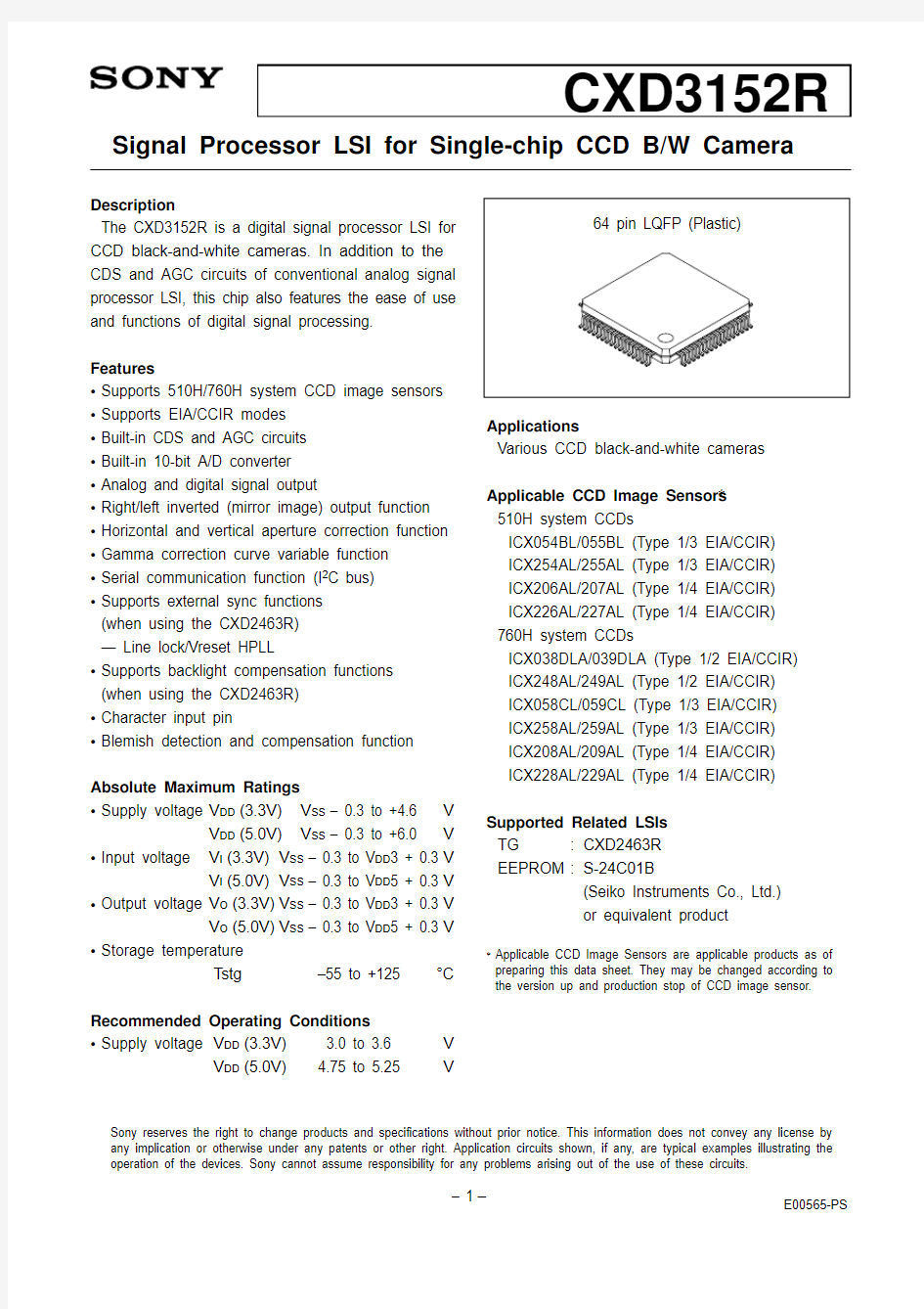
64 pin LQFP (Plastic)
– 2–
A N A , A N A B
C H A R A
M I R R O R
R E F H ,R E F L
R E F H I N ,R E F L I N
M O N I T O R
C A P Y O G O I R I S O C C
D S H P S H D
2M C K I
C S Y N C _I N
C C
D ,
E I A
B L
C W 1, 2
A G C , D G C
S D A , S C L , R E G R E S
Y 0 t o Y 7
P R E F , C V R E F , C O M P
C A P 1, C A P A 2
B l o c k D i a g r a m
Description of Functions by Block
CDS & AGC
?CDS
V DD1 = 5.0V
SHD/SHP external input:
Brightness signal output for iris detection:
?AGC
V DD2 = 5.0V
AGC gain variable range: 8 to 22dB (typ.)
The gain is controlled by the 8-bit DAC for DC voltage generation.
Manual setting possible by the register
A/D Converter
?ADC
10 bits
V DD3 = 3.3V
The input block clamp circuit pulse is generated internally, and external input is impossible.
Built-in voltage follower for the reference voltage
Digital Signal Processing
?DGC
DGC (digital gain control) operates at the maximum AGC (analog gain control) gain.
The gain can be controlled from 0 to approximately 8 times.
The aperture signal coring level is automatically controlled in conjunction with the gain.
?MIRROR
Right/left inverted output possible
?APCON
Horizontal and vertical aperture correction circuit
The circuit can be turned on and off by the setting pin.
Fine adjustment possible by the register
The position at which the aperture correction signal is added can be switched to before or after gamma.?Gamma correction
4 patterns can be selected by the setting pins.
7-line approximation
Adjustable by the register
?Oversampling
Sampling frequency selectable from 2MCKI or (2MCKI/2)
?PED
Standard setting: 7.5 IRE
Adjustable by the register
?Character input
A 1-bit signal from an external pin can be added to the luminance signal.
The gain can be set by the register.
?Blemish detection and compensation function
Up to a total of 10 white point blemishes can be detected and compensated during dark signal. Blemish addresses can be read out by serial communication.
?Digital output
8-bit digital signal output
– 3–
D/A Converter
?DAC
9 bits
V DD6 = 3.3V
Supports –40 to +130 IRE output
Timing Generation
?Timing
Generation of various DSP internal signal processing pulses
Input clock frequencies:
EIA (510 ×492): 19.0699MHz
CCIR (500 ×582): 18.9375MHz
EIA (768 ×494): 28.63636MHz
CCIR (752 ×582): 28.375MHz
Slave operation according to the sync signal
Gain Control
?Gain control
Built-in auto gain control circuit
The maximum AGC (analog gain control) and DGC (digital gain control) gains can be set individually by the registers.
AGC and DGC can be turned on and off individually by external pins.
The gain control time constants can be set by the registers.
Supports backlight compensation
Registers
?I2C bus
Various register settings:
Slave address: [A6:A0] = 0011111 (b)
Related pins:
?External EEPROM
An EEPROM which supports the I2C bus can be connected.
Register values can be automatically read out during power-on.
– 4–
– 5–
V D D 1 (5V )
C C
D I N
C A P 1
C A P A 2
I R I S O U T
Y O U T
Y I N
C A P B 2
V S S 1
M O N I T O R
V S S 2
V D D 2 (5V )
R E F H I N
R E F L I N
R E F H
R E F L
Y 4
Y 3
Y 2
Y 1
Y 0
O E B
S C L
S D A
R E G R E S
A N A
A N A B
R R E F
V D D 6 (3.3V )
V S S 6
C O M P
C V R E F
V SS 5MCKPHS GAMMA2GAMMA1APCON MIRROR DGC AGC V DD 5 (3.3V)DEFECT TEST V SS 4V DD 4 (3.3V)REFBIAS V DD 3 (3.3V)V SS 3
V SS 7Y5Y6Y7MCKO CHARA 2MCKI V DD 7 (3.3V)EIA CCD CSYNC_IN BLCW1BLCW2SHD SHP GOUT
Pin
No.
Symbol I/O Description
1 2 3 4 5 6 7 8 9 10 11 12 13 14 15 16 17 18 19 20 21 22 23 24 25 26 27 28 29 30V DD1
CCDIN
CAP1
CAPA2
IRISOUT
YOUT
YIN
CAPB2
V SS1
MONITOR
V SS2
V DD2
REFHIN
REFLIN
REFH
REFL
V SS3
V DD3
REFBIAS
V DD4
V SS4
TEST
DEFECT
V DD5
AGC
DGC
MIRROR
APCON
GAMMA1
GAMMA2
P
I
O(A)
O(A)
O(A)
O(A)
I(A)
I(A)
P
O(A)
P
P
I(A)
I(A)
O(A)
O(A)
P
P
O(A)
P
P
I
I
P
I
I
I
I
I
I
Analog power supply (5.0V)
Image signal input from CCD
CDS DC bias output
Connect to GND via an approximately 0.1μF capacitor.
Gain control amplifier DC bias output
Connect to GND via an approximately 0.1μF capacitor.
Image signal output for iris detection
AGC image signal output
Image signal input to ADC
Normally input YOUT via an approximately 0.01μF capacitor.
ADC input clamp level (DC) input
High reference (REFHIN) reference level
Analog GND
Output for monitoring the signal input to ADC
Analog GND
Analog power supply (5.0V)
ADC high reference input
ADC low reference input
ADC high reference output
Connect to GND via an approximately 0.1μF capacitor.
ADC low reference output
Connect to GND via an approximately 0.1μF capacitor.
Analog GND
Analog power supply (3.3V)
ADC DC bias output
Connect to GND via an approximately 0.1μF capacitor.
Digital power supply (3.3V)
Digital GND
Test pin. Normally fix high.
Blemish compensation function switching 0: Off, 1: On
Digital power supply (3.3V)
Analog gain switching 0: Fixed, 1: Auto
Digital gain switching 0: Fixed, 1: Auto
Mirror inversion switching 0: Standard, 1: Mirror
Aperture correction switching 0: Off, 1: On
Gamma correction characteristics switching
00: 0.45, 01: 0.6 (register setting), 10: 1.0, 11: S curve
– 6–
No.
Symbol I/O Description
31 32 33 34 35 36 37 38 39 40 41 42 43 44 45 46 47 48 49 50 51 52 53 54 55 56 57 58 59
62MCKPHS
V SS5
CVREF
COMP
V SS6
V DD6 (3.3V)
RREF
ANAB
ANA
REGRES
SDA
SCL
OEB
Y0
Y1
Y2
Y3
Y4
V SS7
Y5
Y6
Y7
MCKO
CHARA
2MCKI
V DD7
EIA
CCD
CSYNC_IN
SHD
I
P
O(A)
O(A)
P
P
O(A)
O(A)
O(A)
I?
I/O?
I/O?
I
O
O
O
O
O
P
O
O
O
O
I?
I?
P
I?
I?
I?
I?
2MCKI input polarity switching
0: Through, 1: Inverted
Digital GND
DAC reference voltage output
Connect to GND via 0.1μF.
DAC phase compensation. Connect to GND via 0.1μF.
Digital GND
Digital power supply (3.3V)
DAC reference voltage generation
Normally connect to GND via 3.3k?.
DAC negative output. Normally connect to GND via 200?.
DAC positive output. Normally connect to GND via 200?.
Register reset. All registers reset to the default when low.
I2C bus data line
I2C bus clock line
Digital output (Y0 to Y7) control.
0: Output, 1: Hi-Z
Digital signal output (LSB)
Digital signal output
Digital signal output
Digital signal output
Digital signal output
Digital GND
Digital signal output
Digital signal output
Digital signal output (MSB)
Y0 to Y7 latch clock output
Character signal input
Reference clock input
Digital power supply (3.3V)
TV mode switching 0: EIA, 1: CCIR
CCD number of horizontal pixels switching
0: 510H system, 1: 760H system
Composite sync input
Backlight compensation window switching
00: Full-screen photometry, 01: Bottom photometry
10: Center photometry, 11: Bottom + center photometry
Data block sampling pulse input
60 61
I?
I?
BLCW1
BLCW2
– 7–
No.
Symbol I/O Description
63 64SHP
GOUT
I?
O(A)
Precharge block sampling pulse input
AGC gain control voltage output (DAC output)
Connect to GND via an approximately 0.1μF capacitor.
Note 1)Asterisks (?) indicate that either 3.3V or 5.0V input is possible. Note 2)The I/O column symbol meanings are as follows.
I: Digital input
O: Digital output
I/O: Digital input/output
I(A): Analog input
O(A): Analog output
P: Power supply/GND
– 8–
– 9–
Logic Block Electrical Characteristics DC Characteristics 3.3V Block
(V DD = 3.0 to 3.6V, V SS = 0V)
Note 1)The applicable pins correspond to the following symbols.
?1AGC, APCON, BLCW1, BLCW2, CCD, CHARA, MCKPHS, CSYNC_IN, DEFECT, DGC, EIA, GAMMA1,GAMMA2, 2MCKI, MIRROR, TEST, OEB (input)?2REGRES
?3MCKO, Y0 to Y7 (output)?4SCL, SDA (I/O)
Note 2)The ANA, ANAB, COMP, CVREF, REFBIAS, REFH, REFL and RREF pins are not included in the DC
characteristics.
Note 1)The applicable pins correspond to the following symbols. ?5SHD, SHP (input)
Note 2)The CAP1, CAPA2, CAPB2, CCDIN, REFHIN, REFLIN, YIN, GOUT, IRISOUT, MONITOR and YOUT
pins are not included in the DC characteristics.
Item
Input high level voltage Input low level voltage Input high level voltage Input low level voltage Output low level voltage Output high level voltage Output low level voltage Input leak current Output leak current
Symbol V IH V IL V IH V IL V OL V OH V OL I IL I OZ
Conditions
CMOS supported
CMOS Schmitt supported I OL = 4mA I OH = –4mA I OL = 4mA V I = V DD , V SS
At high impedance output
Min.0.7V DD —0.75V DD
——V DD – 0.8
—–10–10
Typ.—————————
Max.—0.2V DD —0.15V DD
0.4—0.4+10+10
Unit V V V V V V V μA μA
Applicable pins
?1?2, ?4?4?3?1, ?2, ?4?3, ?4
Item
Input high level voltage Input low level voltage Input leak current
Symbol V IH V IL I IL
Conditions
CMOS supported V I = V DD , V SS
Min.0.7V DD —–10
Typ.———
Max.—0.3V DD +10
Unit V V μA
Applicable pins
?5?5
5.0V Block
(V DD = 4.75 to 5.25V, V SS = 0V)
AC Characteristics(Output load: C L= 50pF)
Item
CSYNC_IN fall setup time, activated by the falling edge of 2MCKI CSYNC_IN fall hold time, activated by the falling edge of 2MCKI Delay time from the falling edge of 2MCKI to MCKO output CSYNC_IN fall setup time, activated by the rising edge of 2MCKI CSYNC_IN fall hold time, activated by the rising edge of 2MCKI Delay time from the rising edge of 2MCKI to MCKO output CHARA setup time, activated by the falling edge of MCKO CHARA hold time, activated by the falling edge of MCKO
Delay time from the falling edge of MCKO to Y0 to Y7 output Power-on reset time
Reset pulse width
SCL clock frequency
SCL clock high level width
SCL clock low level width
SDA setup time, activated by the rising edge of SCL
SDA hold time, activated by the falling edge of SCL
Delay time from the falling edge of SCL to SDA low level output Delay time from the falling edge of SCL to SDA output floating SHP rise time, activated by the falling edge of 2MCKI
SHD rise time, activated by the falling edge of 2MCKI Symbol
t su1
t hd1
t dly1
t su2
t hd2
t dly2
t su3
t hd3
t dly3
t por
t rst
fscl
t high
t low
t su4
t hd4
t dly4
t dly5
t dly6
t dly7
Min.
10
10
—
10
10
—
20
—
1
1
—
700
700
30
—
—
—
Typ.
—
—
—
—
—
—
—
—
—
—
—
—
—
—
—
—
—
—
—
—
Max.
—
—
20
—
—
20
—
—
15
—
—
500
—
—
—
—
20
15
—
30
Unit
ns
ns
ns
ns
ns
ns
ns
ns
ns
μs
μs
kHz
ns
ns
ns
ns
ns
ns
ns
ns
– 10–
– 11–
Master Clock Generation Timing (1) MCKPHS = low
(2) MCKPHS = high
2MCKI
CSYNC_IN
MCKO
2MCKI
CSYNC_IN
MCKO
Video Signal related Input/Output Timing
MCKO
CHARA
Y0 to Y7
– 12–
Reset Timing
V DD
REGRES
I 2C bus Timing
SCL
SDA (output)
SDA (input)
Analog Signal Processing Sampling Pulse Timing
2MCKI
SHP SHD
ADCLK
Note 1)When MCKPHS = low
– 13–
Analog Block Electrical Characteristics 10-bit A/D Converter Electrical Characteristics
(V DD 3 = 3.3V, V SS = 0V, Ta = 25°C)Item
Symbol Min.Typ.Max.Unit Test conditions
DC accuracy DC accuracy
Resolution
Conversion frequency Nonlinearity error
Differential nonlinearity error
RES Fs I.L.D.L.
————
—15——
1020±2.0±1.0
Bits MSPS LSB LSB
Item
Symbol Min.Typ.Max.Unit Test conditions
DC accuracy DC accuracy
Resolution
Conversion frequency Zero scale output voltage Full scale output voltage Full scale output current Nonlinearity error
Differential nonlinearity error
RES Fs V ZERO V FULL I FULL I.L.D.L.
——–151.210——
——01.306.6——
1020.0151.4316.5±2.0±1.0
Bits MSPS mW V mA LSB LSB
?For the test circuit conditions, refer to the Analog Characteristics Test Circuit.?For the power supply names, refer to the symbols in the Pin Description.
9-bit D/A Converter Electrical Characteristics
(V DD 6 = 3.3V, V SS = 0V, Ta = 25°C)?For the test circuit conditions, refer to the Analog Characteristics Test Circuit.?For the power supply names, refer to the symbols in the Pin Description.
– 14–
Item
Symbol Min.Typ.Max.Unit Test conditions CAP1 output DC level CCDIN = 1.6V (DC)GOUT = 1.5V
CAPA2 output DC level CCDIN = 1.6V (DC)GOUT = 1.5V YOUT output DC level CCDIN = 1.6V (DC)GOUT = 2.5V
GCOF1 = V4 – CDSDC V4 = YOUT output DC level CCDIN = 1.6V (DC)GOUT = 1.5V
GCOF2 = V5 –CDSDC V5 = YOUT output DC level CCDIN = 1.6V (DC)GOUT = 0.5V YOUT output gain CCDIN = S1 (Note 2)GOUT = 3.3V YOUT output gain CCDIN = S1 (Note 2)GOUT = 0V
YOUT output AC level CCDIN = S1 (Note 3)GOUT = 0.5V YOUT output AC level CCDIN = S1 (Note 3)GOUT = 2.5V IRISOUT DC level CCDIN = 1.6V (DC)GOUT = 3.3V IRISOUT gain
CCDIN = S2 (Note 4)GOUT = 3.3V IRISOUT AC level CCDIN = S2 (Note 5)GOUT = 3.3V
CAP1 DC level
CAPA2 DC level CDS DC level AGC DC offset 1AGC DC offset 2AGC minimum
gain characteristics (Note 1)AGC maximum
gain characteristics (Note 1)
AGC D range 1AGC D range 2IRIS DC level IRIS gain IRIS D range CAP1
CAPA2CDSDC GCOF1GCOF2AGCG1AGCG2AGCD1AGCD2IRISDC IRISG IRISDR 1.5
2.52.9–0.2–0.4
3.315.71.91.61.68.31.6 1.6
3.03.4006.418.82.22.02.29.52.1 1.7
3.53.90.20.48.721.12.72.72.610.72.7V
V
V
mV
mV
dB
dB
V
V
V
dB
V
?For the test circuit conditions, refer to the Analog Characteristics Test Circuit.?For the power supply names, refer to the symbols in the Pin Description.Note 1)Refer to the AGC Gain Characteristics.
Note 2)S1: Va = 100 to 400mV, Vb = 1.6V (Va = peak to peak, Vb = peak to GND)Note 3)S1: Va = 1000mV, Vb = 1.6V Note 4)S2: Va = 400mV, Vb = 1.6V Note 5)S2: Va = 1000mV, Vb = 1.6V
– 15–
Item
Symbol Min.Typ.Max.Unit Test conditions CAPB2 output DC level SW1 = A, SW2 = A MONITOR output DC level CLP = "H"
SW1 = A, SW2 = A MONITOR output gain SW1 = B, SW2 = B YIN = S4 (Note 1)
MONITOR output AC level SW1 = B, SW2 = A YIN = S3 (Note 2)
CAPB2 DC level
CLP DC level CLP gain CLP D range CAPB2
CLPDC1CLPG CLPD 2.6
2.602.0 2.7
2.70.62.4 2.8
2.81.22.7V
V
dB
V
?For the test circuit conditions, refer to the Analog Characteristics Test Circuit.?For the power supply names, refer to the symbols in the Pin Description.Note 1)S4: Va = 1000mV, Vb = 2.75V (Va = peak to peak, Vb = peak to GND)Note 2)S3: Va = 2000mV, Vb = 3.6V
OPAMP Electrical Characteristics
(V DD 1, 2 = 5.0V, V DD 3 = 3.3V, V SS = 0V, Ta = 25
°C)Item
Symbol Min.Typ.Max.Unit Test conditions REFH output DC level SW1 = A, SW2 = A REFL output DC level SW1 = A, SW2 = A
OPAMP DC H OPAMP DC L
OPH OPL
2.80.8
2.90.9
3.01.0
V V
?For the test circuit conditions, refer to the Analog Characteristics Test Circuit.?For the power supply names, refer to the symbols in the Pin Description.
AGC Gain Characteristics (V DD 1, 2 = 5.0V, V DD 3 = 3.3V, V SS = 0V, Ta = 25°C)
25201510A G C g a i n [d B ]
500
0.5
1.0
1.5
2.0
GOUT voltage [V]
2.5
3.0
3.3
AGC Gain Characteristics
– 16–
A n a l o g C h a r a c t e r i s t i c s T e s t C i r c u i t
0.1μF 0.1μF
0.1μF 0.1μF
Analog Input/Output Pin Equivalent Circuits
– 17–
– 18–
Note)For the power supply names in the equivalent circuits, refer to the symbols in the Pin Description.
– 19–
Timing Chart
Horizontal Direction Timing
2MCK:Master clock input for the CXD3152R
MCK:Internal reference clock produced by dividing the input reference clock (2MCK) in half.
MCKO:Latch clock for digital output signal (Inverted MCK signal)
CCDIN:Imaging signal from CCD
SHP:Precharge level sampling pulse input
SHD:Video level sampling pulse input
cblk:Internal composite blanking pulse (for VIDEO output signal)
CSYNC:Composite sync pulse input (in phase for CSYNC_IN and the VIDEO output signal) A_CLP:Internal pulse for analog clamp
D_CLP:Internal pulse for digital clamp
DOUT[7:0]:8-bit digital output signal
ANA:Analog output signal
Vertical Direction Timing
HD:Internal horizontal sync signal
cblk:Internal composite blanking pulse (for VIDEO output signal)
CSYNC:Composite sync pulse input (in phase for CSYNC_IN and the VIDEO output signal) A_CLP:Internal pulse for analog clamp
D_CLP:Internal pulse for digital clamp
CCDIN:Video signal from the CCD
DOUT[7:0]:8-bit digital output signal
– 20–