MEMORY存储芯片TMS27C512JL中文规格书

TPC10 SERIES
CMOS FIELD-PROGRAMMABLE GATE ARRAYS
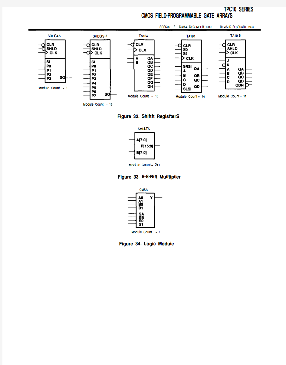
SRFS001 F -D3864, DECEMBER 1989 -REVISED FEBRUARY 1993 SREG4A SREGS A TA164 TA194 TA195
Module Count = 8
Module Count = 18 Module Count= 14 Module Count= 11
Module Count = 18
Figure 32. Shift Registe『S
SMULTS
M创ule Count= 241
Figure 33. 8-Blt Multiplier
CMSA
Module C口unt= 1
Figure 34. Logic Module
TPC10 SERIES CMOS FIELD-PROGRAMMABLE GATE ARRAYS
SRFS001 F -D3864, DECEMBER 1989 -REVISED FEBRUARY 1993
package pin assignments (continued)
2主45____§_ 7 8 9 10 11
AHRM HR -』0000000000000000000000。。。000 。。。。
。。O O O :T O P V I E 明l 1000000 000 000 000 00 00 。。
000 。。0000000000000000000000I /。Pin Assignments for the 84-Pin Ceramic Pin Grid Array Package SIG NAL
TPC1010A TPC1020A PRA
A11 A11 PRB
B10 B10 MOD E
E11 E11 SDI
B11 B11 DCL K
C10 C10 V pp
K2 K2 CLKor 1/0
F9 F9 GND
B7, E 2, E 3, K5, F10, G 10 B7, E 2, E 3, K 5, F 10, G 10 V ee
B5,F1,G2,K7,E9,E10
B5,F1,G2,K7,E9,E10 Ne {No internal connecti 。n)B1, B 2, e 1, e 2, K 1, J 2, L 1,
B2 J10, K 10, K 11, e 11, D10, D 11
NOTES: A. All pins marked GND are ground connections and must be connected t 。circuit ground
B. I/pp must be terminated to V ee except during programming.
e. P再A and PRB, t he diagnostic probe口utputs,sh 。uld remain open if not used as I/Os
D. MODE must be terminated to circuit ground except during programming.t
E. SDI and DeLK should be terminated to circuit ground during normal 。peration if not used as I/Os .
t F . Unused 1/0 pins are automatically designated by the Action Logic System as outputs and should remain unconnected. Unused 1/0 pins are driven low by design.
G. All unidentified pins on the pin assignment drawings are standard I/Os.
t H. Orientation pin e3 is connected internally to pin e2. The security fuse must be programmed for SDI and DeLK to function as I/Os. For device debugging 。
n the user ’s circuit board, M ODE, S DI, and DeLK should be terminated to circuit ground through a 10-kU {or greater) resistor. They can be tied to ground if not debuggi『1g.Figure 38. 84-Pin CPGA Pin Assignment