2013-Reconfigurable antennas
Reconfi gurable Antennas
Randy L. Haupt and Michael Lanagan
Haupt Associates
8493 Baseline Rd, Boulder, CO 80303 USA
Tel: +1 (303) 736-8132; E-mail: haupt@https://www.sodocs.net/doc/cd7706794.html,
The Pennsylvania State University
263 Materials Research Laboratory, University Park, PA 16802 USA
Tel: +1 (814) 865-6992; Fax: +1 (814) 865-2326; E-mail: mxl46@https://www.sodocs.net/doc/cd7706794.html,
Abstract
Recon? gurable antennas change polarization, operating frequency, or far-? eld pattern in order to cope with changing system parameters. This paper reviews some of the past and current technology applicable to recon? gurable antennas, with several examples of implementations. Mechanically movable parts and arrays are discussed, as well as more-recent semiconductor-component and tunable-material technologies applicable to recon? gurable antennas. Keywords: Recon? gurable antennas; recon? gurable arrays; antenna arrays; wideband antennas; re? ector antennas; microstrip patch antennas
1. Introduction
T o confi gure means to arrange or organize the parts of
something to achieve a purpose. For instance, confi guring a microstrip antenna consists of determining the patch shape, substrate parameters, type and location of the feed, etc., in order for the antenna to radiate at a desired frequency and polarization. If the desired operating characteristics of the antenna change, then the antenna must be reconfi gured or rebuilt to meet the new specifi cations. Reconfi gurable anten-nas change their performance characteristics by altering the current fl ow on an antenna, using mechanically movable parts, phase shifters, attenuators, diodes, tunable materials, or active materials. A reconfi gurable antenna can be a single antenna or an array.
A reconfi gurable antenna modifi es the antenna’s pattern, polarization, or frequency/bandwidth in some desirable fash-ion. For instance, a reconfi gurable antenna might steer or place a null in an antenna’s pattern, switch from right-hand circularly polarized to left-hand circularly polarized, or move the resonant frequency from 2 GHz to 2.4 GHz. In this way, a single antenna replaces two or more antennas, in order to achieve multiple goals. Arrays are the ultimate reconfi gurable antenna, because they have many avenues for controlling the current across the aperture. A reconfi gurable array may have reconfi gurable elements, or a reconfi gurable array may change the amplitude and phase of each element, the number of active elements, the elements’ positions, or the polarization.
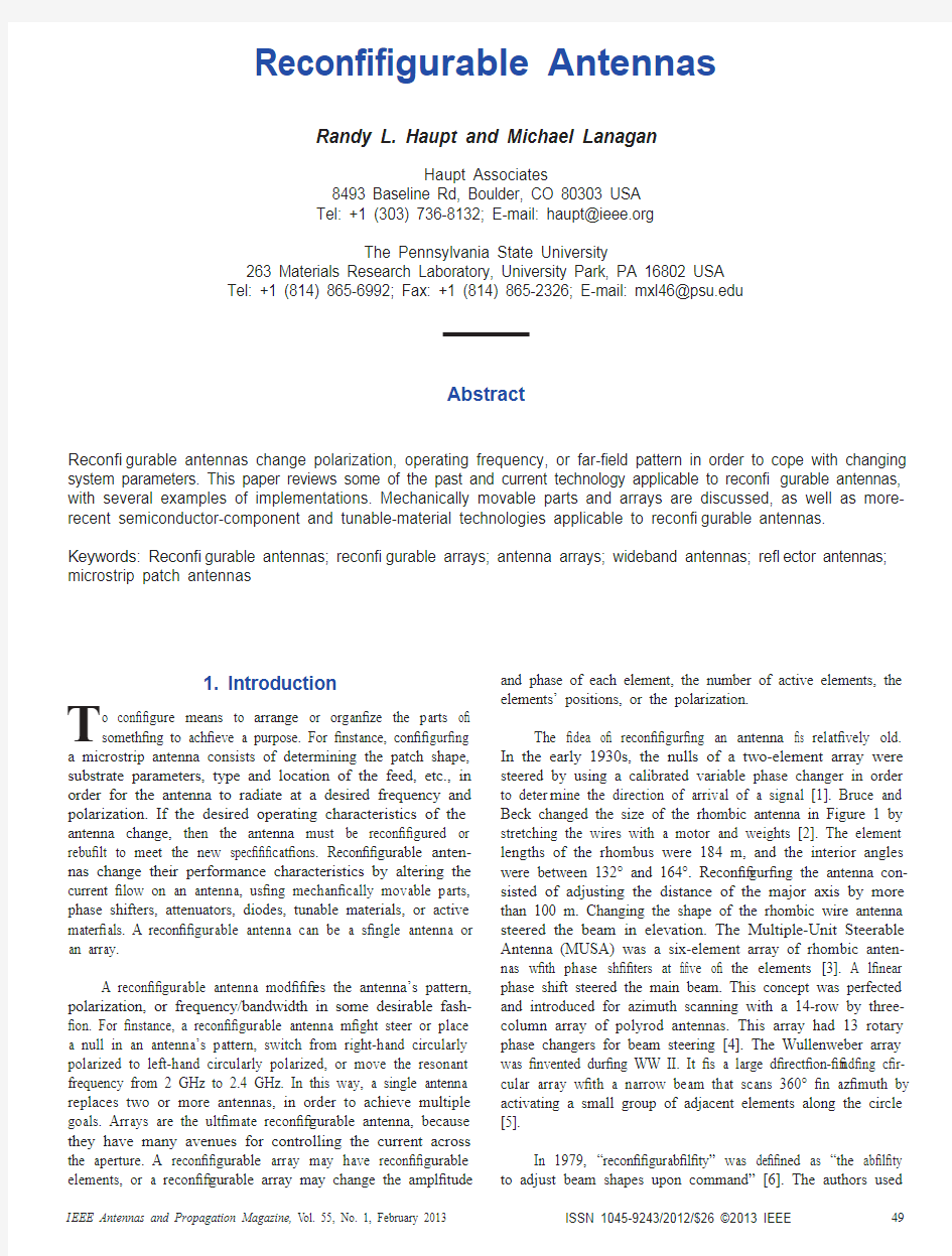
The idea of reconfi guring an antenna is relatively old. In the early 1930s, the nulls of a two-element array were steered by using a calibrated variable phase changer in order to deter m ine the direction of arrival of a signal [1]. Bruce and Beck changed the size of the rhombic antenna in Figure 1 by stretching the wires with a motor and weights [2]. The element lengths of the rhombus were 184 m, and the interior angles were between 132° and 164°. Reconfi guring the antenna con-sisted of adjusting the distance of the major axis by more than 100 m. Changing the shape of the rhombic wire antenna steered the beam in elevation. The Multiple-Unit Steerable Antenna (MUSA) was a six-element array of rhombic anten-nas with phase shifters at fi ve of the elements [3]. A linear phase shift steered the main beam. This concept was perfected and introduced for azimuth scanning with a 14-row by three-column array of polyrod antennas. This array had 13 rotary phase changers for beam steering [4]. The Wullenweber array was invented during WW II. It is a large direction-fi nding cir-cular array with a narrow beam that scans 360° in azimuth by activating a small group of adjacent elements along the circle [5].
In 1979, “reconfi gurability” was defi ned as “the ability to adjust beam shapes upon command” [6]. The authors used
a six-beam antenna to dynamically change the coverage area for a communications satellite. Several additional papers reported other reconfi gurable space-based arrays. In the 1990s, a research group in England described their efforts to alter the refl ecting surface of a parabolic-refl ector antenna in order to control the radiation pattern [7]. From the mid-1990s until the present, reconfi gurable-antenna projects have mostly involved microstrip antennas, and various semiconductor technologies applied to altering the current fl ow on the microstrip antenna. Bernhard wrote an excellent overview of reconfi gurable antennas, with many examples [8].
This paper is an introduction/tutorial on reconfi gurable-antenna technology. It begins with the oldest technology, mechanically movable parts and arrays, and then transitions to the more-recent semiconductor-component and tunable-mate-rial technologies. A detailed explanation of the technology with background information and examples are given. Some of the interesting material technologies, such as active materi a ls, are promising for reconfi gurable antennas with low loss at high frequencies.
2. Mechanically Movable Parts
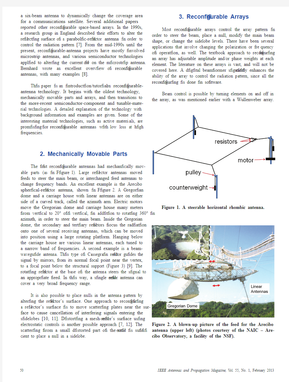
The fi rst reconfi gurable antennas had mechanically mov-able parts (as in Figure 1). Large refl ector antennas moved feeds to steer the main beam, or interchanged feed antennas to change frequency bands. An excellent example is the Arecibo spherical-refl ector antenna, shown in Figure 2. A Gregorian dome and a carriage house with linear antennas are on either side of a curved track, called the azimuth arm. Electric motors move the Gregorian dome and carriage house many meters from vertical to 20° off vertical, in addition to rotating 360° in azimuth, in order to steer the main beam. Inside the Gregorian dome, the secondary and tertiary refl ectors focus the radiation onto one of several receiving antennas, which can be moved into position using a large rotating platform. Hanging below the carriage house are various linear antennas, each tuned to a narrow band of frequencies. A second example is a beam-waveguide antenna. This type of Cassegrain refl ector guides the signal by mirrors, from its normal focal point near the vertex, to a focal point below the structural support (Figure 3) [9]. The rotating refl ector at the base of the antenna steers the signal to an appropriate feed. In this way, a single refl ector antenna can cover a very broad frequency range.
It is also possible to place nulls in the antenna pattern by altering the refl ector’s surface. One approach to reconfi guring a refl ector’s surface is to move scattering plates near the sur-face to cause cancellation of interfering signals entering the sidelobes [10, 11]. Distorting a mesh-refl ector’s surface using electrostatic controls is another possible approach [7, 12]. The scattering from a small distorted part of the refl ector is suffi -cient to place a null in a sidelobe.
Figure 1. A steerable horizontal rhombic antenna.
Figure 2. A blown-up picture of the feed for the Arecibo
antenna (upper left) (photos courtesy of the NAIC – Are-cibo Observatory, a facility of the NSF).
3. Reconfi gurable Arrays
Most reconfi gurable arrays control the array pattern in
order to steer the beam, place a null, modify the main beam shape, or change the sidelobe levels. There have been several applications that involve changing the polarization or fre q uency of operation, as well. The textbook approach to recon fi guring an array has adjustable amplitude and/or phase weights at each element. The literature on these arrays is vast, and will not be covered here. A digital beamformer signifi c antly enhances the ability of the array to control the radiation pattern, since all the reconfi guring is done in software. Beam control is possible by turning elements on and off in the array, as was mentioned earlier with a Wullenweber array.
Figure 4 shows this concept extended to a spherical array that was implemented on a geodesic dome. Each triangle on the dome was a subarray [13]. The active aperture was formed by combining the outputs from adjacent subarrays. Including more subarrays expanded the original active aper t ure (Figure 4). The active aperture could be moved to another location on the dome in order to point the main beam in a dif f erent direction. Other reconfi gurable arrays that make use of switching an element on and off include dynamically thinning an array as one way to alter the sidelobe levels and nulls in order to reject interference [14], and time-modulated arrays that lower the average sidelobe levels by quickly switching elements on and off, with on times proportional to the desired amplitude of the element weight [15].
Figure 3. A diagram of a beam-waveguide antenna.
Figure 4. A phased array built on a geodesic dome. The yellow regions represent regions of activated subarrays. Another approach to reconfi guring an array is to physi-cally move elements. Some very large refl ector-antenna arrays use this concept. For instance, the Atacama Large Millime-ter/sub-millimeter Array, or ALMA, will be a radio telescope composed of 66 12 m and 7 m parabolic dishes in Chile’s Andes Mountains (Figure 5) [16]. The telescope will operate at frequencies from 31.25 GHz to 950 GHz. Array confi gura t ions from 250 m to 15 km will be possible. The ALMA antennas will be moved between fl at concrete slabs by a spe c ial vehicle, as shown in Figure 5. A second example is the Very Large Array (VLA) radio telescope in New Mexico, built from 27 dish antennas that are 25 m in diameter [17]. Elements are placed in a Y shape, and can be changed by moving the elements along a railroad track (Figure 6). Four possible confi gurations, with aperture sizes of 36 km, 10 km, 3.6 km, or 1 km, are used. The array can operate between 73 MHz and 50 GHz.
The idea of moving elements to form a desired array aper-ture also extends to space. For instance, the TechSat 21 project investigated creating a large sparse antenna array by placing antenna elements on small spacecraft, and assembling the aperture with a formation of the satellites [18]. Beam for m ation was a function of the satellite constellation and the weighting of the signals.
Figure 5. An artist’s concept of ALMA (ESO/NAOJ/NRAO).
Figure 6. The VLA antennas on railroad tracks (NRAO/AUI/NSF).
4. RF Switches
An RF switch serves to open or close a current path on a reconfi gurable antenna. A popular way to build a reconfi gur a ble antenna is to connect various pieces of the antenna with RF switches. Opening and closing switches guides the current in a desirable path that changes the antenna’s radiation prop e rties, as well as its impedance.
RF switches may be mechanical or semiconductor. A switch is an open circuit when no actuation voltage is applied, and a low-impedance path for the RF signal when an actuation voltage is applied. The switch can be implemented in a series or shunt confi guration. Some important characteristics of a switch are [19]:?
Characteristic impedance: if the switch is non-refl ec-tive, then it is matched to the transmission path; otherwise, it is refl ective. The VSWR or return loss indicate the degree of matching.
? Bandwidth: some switches are low-pass fi lters (pass dc), while others are bandpass fi lters.? Topology: is the switch normally on or off??
Insertion loss and isolation: the ratio between the switch’s output and input powers when the switch is on and off, respectively.
?
Switching speed: the on time for a switch is defi ned by the time from when the control pulse reaches 50% of its level to the time that the RF signal is at 90% of its peak. The off time for a switch is defi ned by the time from when the control pulse reaches 50% of its level to the time that the RF sig n al is at 10% of its peak. Switching time is the lar g er of the on and off switch times.
? Expected life time: measured in number of switch actuations until failure.
?
Power handling: measured in watts.
Below microwave frequencies, a low-pass switch acts like
a resistor (on R ) when on, and a capacitor (off C ) when off. In contrast, a bandpass switch behaves like one capacitor when on, and a different capacitor when off. As the frequency increases, the ground inductance, bond-wire inductance, and transmission-line properties become signifi cant factors, and complicate the circuit model. Parasitic resistances in the switch limit the upper-frequency bound. A switch fi gure-of-merit (FOM) is the cutoff frequency [20]:
1c off on
f π=
. (1)
A rule of thumb for the highest operating frequency for the switch is approximately 10c f [21].
The switching speeds of semiconductor switches are of the order of nanoseconds, while the switching speeds of mechanical switches are of the order of milliseconds. System constraints may limit the type of switch used, based on required switching times.
Switches can be used to reconfi gure microstrip-patch antennas in several different ways. For instance, Figure 7 shows a two-dimensional array of metal patches on a substrate [22]. The sides of adjacent patches are connected with RF switches, in order to confi gure a desirable patch antenna. Fig u re 8 is an example of a patch with slots that can be shorted, in order to switch between polarizations [23].
Figure 8. A recon? gurable slotted-patch antenna.
Figure 7. Recon? gurable microstrip patches.
4.1 Semiconductor Switch
Figure 9 is a diagram of a fi eld-effect transistor (FET) switch. Increasing the voltage at the gate increases the con-ducting channel’s size beneath the gate, and allows current to fl ow between the source and drain. FET switches come in sev e ral varieties. Metal-semiconductor fi eld-effect transistor (MESFET) and pseudomorphic high-electron-mobility tran-sistor (PHEMT) switches are two variations, which are com-pared in Table 1. The authors in [24] suggested using FET switches in a confi guration similar to Figure 7. The RF switch array was controlled with a light-emitting-diode backplane, which isolated the control circuitry from the RF paths in the antenna.
Another widely used microwave switch is the PIN diode [25]. It has heavily doped p-type and n-type regions (used for ohmic contacts), which are separated by a wide, lightly-doped intrinsic region (Figure 10). Forward biasing a PIN diode cre-ates a very low resistance at high frequencies, while reverse biasing results in an open circuit. The PIN diode is current controlled, and can handle one or more amps of RF current. The authors in [23] suggested using PIN-diode switches for the confi guration in Figure 8. Table 1 compares the characteristics of FET and PIN-diode switches. Some notable differences between the two types of switches are [26, 27]:?
PIN diodes are current controlled, while FETs are voltage controlled. FETs require only a voltage signal for switching, instead of a dc current. This means that they have essentially zero dc power consumption, compared to the 10 mW or so it takes to turn on a PIN diode.
?
PIN diodes have the ability to control large RF sig-nal power while using much smaller levels of con-trol power.
?
PIN diodes are less susceptible to electrostatic-dis-charge (ESD) damage.
?
The off-capacitance of PIN diodes is a function of reverse voltage: the more negative the voltage, the less capacitance.
? For FETs, the capacitance is not a strong function of reverse voltage.
?
PIN diodes have a higher fi gure-of-merit than FETs. The useful upper-frequency-response limit of PIN diodes can be much higher, due to lower off-state
capacitance (off C ) for a given on resis
t ance (on R ). Recently, a reconfi gurable patch antenna was demon-strated in which the resonant frequency was altered between
2 GHz and 2.25 GHz, when the electrical length of a spiral-shaped slot in the patch was modifi ed by a biased diode [28].
4.2 MEMS Switches
MEMS switches are tiny mechanical switches made on a substrate (silicon, quartz, glass) [29]. Unlike the PIN-diode and FET switches, a MEMS switch is mechanical. Figure 11 shows three types of MEMS switches in their on and off posi-tions. The cantilever beam in Figures 11a and 11b is anchored to a post on the left, while the other end of the beam is sus-pended above the drain. An electrostatic force pulls the beam
Table 1. A comparison of FET and PIN-diode switches [21].
1 μm MESFET
0.25 μm PHEMT
Silicon PIN diode
Number of terminals 332Typical on resistance 1.5 ohm-mm 1.2 ohm-mm 1.7 ohms Typical off capacitance 0.40 pF/mm 0.32 pF/mm 0.05 pF FOM (Eq. 1)265 GHz 414 GHz 1872 GHz Breakdown voltage 15 V 8 V 50 V Lower frequency limit dc dc 10 MHz Driver circuit complexity low low
high
Driver requirements
0 V on; –5 V off
+0.5 V on; –5 V off
5 to 10 mA on; 0 to –30 V off
Figure 9. A diagram of a FET.
down when a voltage is applied, and creates an electrical
path between the beam and the drain. Figures 11c-11f show a
MEMS membrane switch, which consists of a fl exible, thin,
metal membrane, anchored to posts at both ends. A potential
applied to the bias electrode pulls the membrane down and
close s the circuit. An ohmic contact is a metal-to-metal con-
nection, while a capacitive contact has a dielectric between the
two metal contacts. Ohmic switches have a higher bandwidth
than capacitive switches. The capacitive MEMS switches han-
dle higher peak power levels and tolerate environmental effects
better than ohmic contacts. The fi gure-of-merit for MEMS
switches was reported at 9000 GHz [20]. Switching speeds for
electro-statically driven capacitor structures are 10 μs. Recently,
MEMS switches with piezoelectric fi lms have been developed,
and have fast switching times (1-2 μs). The cantilever device
travels 6 μm between the on and off states [30].
MEMS switches have low power consumption, low inser-
tion loss, and high isolation, like mechanical switches, but are
small, light weight, and low cost, like semiconductor switches
[31]. On the other hand, MEMS switches have high losses at
microwave and mm-wave frequencies, limited power-handling
capability (~100 mW), and they may need expensive packaging
to protect the movable MEMS bridges against the environment.
MEMS switches have been proposed for use in reconfi gur-
able antennas since the late 1990s [29]. For exam p le, two ultra-
wideband monopoles with a reconfi gurable band notch in the
wireless-LAN frequency range (5.150 GHz to 5.825 GHz) are
shown in Figure 12 [32]. The antenna was an elliptical patch,
fed with a coplanar-waveguide line. The U-shaped slot was
approximately 2
λ long, and had a frequency notch when the
MEMS switch was open, but not when the MEMS switch was
closed. When the switch was open at 5.8 GHz, the currents in
the inner and outer side of the slot fl owed in opposite directions
and cancelled each other. When the MEMS switch was closed,
the slot was shorted at its center point, so the total length of the
slot was cut in half. Conse q uently, the slot no longer supported
the resonating currents, and radiation occurred as if the slot was
not present.
The second antenna in Figure 12 had two inverted-L-
shaped open stubs that connected and disconnected the stubs
from the elliptical patch via MEMS switches. Shorting the
stubs to the patch created a rejection band. At the resonance
frequency, the direction of the current on the stub fl owed in the
opposite direction to the current along the nearby edge of the
radiator, so the radiated fi elds cancelled. When the stubs were
not shorted, the antenna operated over the whole UWB range
(3.1 GHz to 10.6 GHz) without any rejection band. The MEMS
switches actuated through the RF signal path, without any dc
bias lines that might have complicated the switch’s fabrication
and integration, while degrading the radiation per f ormance due
to RF leakage through the bias.
Reconfi gurable antennas can also change the antenna’s
polarization. For instance, placing MEMS switches in the feeds
of microstrip antennas provides the ability to switch from one
linear polarization to the orthogonal linear polariza t ion, or to
circular polarization, as shown in Figure 13 [33].
Figure 11. Three types of MEMS switches in the on and off
positions.
Figure 10. A diagram of a PIN diode.
Figure 12. A diagram of the recon? gurable U-slot and
L-stub antennas.
MEMS structures are fabricated using a number of tech-niques, including etching trenches in the substrate, or building a multilayer structure on a planar substrate. Future research and development activities will need to address the cost and scalability of the MEMS process for large arrays. There are several important substrate properties that must be controlled, including surface roughness, permittivity, and dielectric loss. Recently, low-cost liquid-polymer substrates with 3r ε= and tan 0.002δ= have been shown to be viable substrates for MEMS devices [34].
5. Varactors
Unlike the PIN diode, a varactor diode has a very thin depletion layer that acts like the insulating dielectric, and the P and N regions that act like the conducting plates (Fig-ure 10). The capacitance is inversely proportional to the square root of the applied voltage, since the thickness of the depletion layer increases with the reverse bias. Varactors have a high-to-low capacitance ratio that is typically six over a voltage change of 0 V to 12 V .
Varactors are useful for tuning the antenna’s frequency range. For instance, varactors were placed at the radiating edges of a microstrip-patch antenna in order to increase its very narrow bandwidth to a bandwidth of about 30% [35]. Strategically placing varactors along a slot antenna produced dual bands, with controllable fi rst and second resonant fre q uencies [36]. A reconfi gurable partially-refl ecting-surface (PRS) antenna was built. It had a measured realized gain that varied from 10 dBi to 16.4 dBi over the tuning range of 5.2 GHz to 5.95 GHz, as the bias voltage was tuned from 6.49 V to 18.5 V [37]. The antenna had a partially-refl ecting-surface material on the top surface, and a phase-agile surface below a microstrip patch. One phase-Figure 13. A recon? gurable antenna that changes polari-zation using MEMS.
agile refl ection cell was a microstrip-patch resonator, with varactor diodes that varied the resonant frequency of the patch antenna’s refl ection phase. The 13.5% tuning range extended the operating-frequency range by six times. The antenna’s tuning bandwidth was lim i ted by the varactor diode’s tuning range for the phase-agile cells, and the antenna’s effi ciency was limited by the varactor diode’s series resistance. A slotted-monopole antenna, modi fi ed with a varactor, could be tuned between 1.6 GHz and 2.3 GHz without a signifi cant change in the antenna’s effi c iency [38]. Radiation pattern control has also been demon s trated using varactors [39].
6. Tunable Materials
Prospective devices with performance rivaling varactors will be based on materials that have tunable electrical, mag-netic, and mechanical properties. For example, the propaga t ion wavelength within the RF structure or impedance will be altered by permittivity (r ε) or permeability (r μ) changes, and the ability to tune the structure will be fundamentally related to the magnitudes of r ε and r μ [40]. Tunable mechanical strain alters either the effective length of the antenna, or modi fi es the impedance through capacitive coupling. Many con c epts, such as tunable permeability, have been previously studied for microwave and millimeter-wave phase shifters [41]. Future tunable materials and devices will advance antenna technology through miniaturization and integration. A representative list of potential technologies for reconfi gurable antennas is summarized in Table 2.
6.1 Tunable Conductivity
Conductivity in semiconductors can be tuned through changes in temperature, bias, or light. The conductivity of a semiconductor varies depending on the bandgap energy and the level of doping, and depending on defects in the material. Shining light with a photon energy greater than the bandgap on an intrinsic semiconductor increases the free-electron and hole-charge carriers, which in turn increases the semiconduc-tor’s conductivity. Solar cells are a good example.
Applying an electric fi eld to a polymer electrolyte-silver-polyaniline composite alters the material from a state of low to high conductivity. Polymer composites with controllable resistance at microwave frequencies have stable, reproducible switching over more than 1000 test cycles [49].
Phase-change chalcogenides, such as 225Ge Sb Te (pro-posed for non-volatile memory applications), also have tun a ble conductivity. Measurements have demonstrated that amorphous chalcogenides maintain low conductivity values into the GHz frequency range [50]. These become conducting upon recrystallization of the amorphous material. Resistivity changes of nearly three orders of magnitude are possible in small structures, by methods involving laser and Joule heating [51].
Silicon is a viable candidate for optically controlling con d uctivity. In [52], the authors reported on creating planar antennas on a silicon wafer by precisely forming plasma chan-nels in the shape of the desired antenna. Varying the conduc-tivity of silicon using an IR LED was reported for a recon-fi gurable patch antenna [53], and for a partially adaptive array with broadband monopoles [54].
6.2 Tunable Permittivity
A number of approaches have been explored to achieve economical solutions for a high ability to tune with low losses and fast response, for the purpose of controlling microwave fi lters and phased arrays. The relative “tunability” of the per-mittivity of a system is defi ned as
()()
()
00r r r r E n εεε?=
, (2)
where ()0r ε and ()r E ε are the small-signal relative permit-tivities without bias and with a bias of strength E [V/cm], respectively. Tunabilities as high as 75% have been reported for 3(Ba,Sr)TiO thin fi lms at 1500 kV/cm [55]. A high elec t ric fi eld is required to generate a large tunability; however, the tuning voltage is low (25 ()()() 2 01max r r Q Q V n K ?= , (3) where Q is the inverse of the device’s loss; ()0Q and ()max Q V are at zero bias and at the maximum voltage, respec t ively; and r n is the tunability from Equation (2). K factors as high as 500 have been reported for paraelectric 3SrTiO thin fi lms on 3SrRuO conductors. Dielectric materials with the highest tunability have paraelectric/ferroelectric transition temperatures that are below the operating temperature. The magnitude of the tunability is directly proportional to the dielectric permittivity, which approaches 1,000 for materials with the highest tunability [58]. The intrinsic dielectric loss increases with frequency, which may be a concern as the operating frequency increases into the mm-wave range [59]. The dielectric permittivities of thin fi lms and bulk materi-als are altered through an externally applied electric fi eld. Large changes in permittivity under a dc voltage bias have been demonstrated in epitaxial paraelectric 0.50.53Ba Sr TiO (“BST”) thin fi lms that are deposited on sin g le-crystal 3LaAlO and MgO sub s trates [42]. The loss of the dielectric fi lm is represented as an average Q value between the zero-fi eld and high-electric-fi eld bias. Bulk BST ceramics offer high tunability, and have higher Q values that BST fi lms. Recent results have shown that high electric fi elds can be applied to bulk ceramics with nanometer-sized grains, corre s ponding to higher high overall tunability [43]. 6.3 Tunable Permeability Similar to the tunable response in dielectric materials, the magnetic permeability decreases with the application of a Table 2. Potential technologies with tunable dielectric, magnetic, and strain response for frequency-agile devices. Method Tunability (%) Q Stimulus Frequency Dielectric Thin Film [42]3045Electric Field 70E =kV/cm 1-20 GHz Dielectric Bulk Ceramic [43]16100 >Electric Field 15E =kV/cm 1-10 GHz Magnetic Film [44]15511 Q < (100 μm)3-7 GHz MEMS variable capacitor [47]80100300Q < 1 μm 0.5-4 GHz Varactor [48] 60 3060 Q < (20 V) 10 GHz *Tunable frequency is proportional to the square root of the tunable permeability or permittivity, and the squares of the values are shown for comparison with the other methods (shown in parenthesis). Table 3. The strain responses of several types of active materials. Actuation Mechanism Piezoelectric Electrostriction Maxwell Magnetostriction Phase Change Materials PZT, PMN-PT single crystal PMN-PT ceramics and PVDF Silicone Terfernol Nitinol % strain range 0.1 to 1.50.1 to 4200.26Reference [69] [70] [71] [72] [72] static fi eld. An early example of a 1.4 cm by 1.8 cm rectangu-lar microstrip patch was printed on a 1.27 mm thick ferrite substrate (Trans-Tech G-113 YIG), and was fed with a coaxial probe near the edge of a long dimension [60]. The center design frequency was 4.6 GHz, which was tunable over a 40% bandwidth when it was magnetically biased in the plane of the substrate, and perpendicular to the resonant dimension. The polarization response of patch antennas on garnet single crys t als has also been studied at 5 GHz for externally applied magnetic fi elds of 600 G. One advantage of higher permeabil-ity over high permittivity is that the effective patch dimensions can be reduced, without sacrifi cing bandwidth [61]. There are fundamental materials limitations for tunable magnetic mate-rials, because the permeability and the highest operating fre-quency are inversely related [62]. Ferrites are a class of high-frequency magnetic materials with low eddy current and hys-teretic losses [63]. Tunable magnetic structures have thin-fi lm and bulk-ceramic forms. Conformal Permalloy fi lms (120 nm thick) were deposited on CMOS structures, having lower conduction and hysteresis losses than bulk NiFe in the GHz frequency range [44]. In addition, eddy-current losses at high frequency were minimized through the inductor’s design. Judicious pat t erning of the magnetic fi lm raises the ferromagnetic reso n ance, and hence the operating frequency, of the tunable thin-fi lm inductors; however, the magnetic-fi lm technology will be limited to frequencies below 10 GHz, because of the limitation in the ferromagnetic resonance frequency. There are funda-mental material limitations for tunable magnetic materials, because the magnitude of r μ and the highest operating fre-quency are inversely related [62]. The magnetic response of ferrites is limited to below the K band [64]. Bulk-ceramic fer-rite plugs were placed within the center of a dielectric resona t or operating in the TE01δ mode [45]. The resonator was placed on top of a coil, which was used to apply the dc mag n etic fi eld. A high Q value was reported because of the low-loss dielectric resonator within the tunable structure. 6.4 Tunable Mechanical Tunable mechanical materials are also known as active materials, and they change shape when exposed to an electric, magnetic, or thermal stimulus. Electrostrictive materials strain under an applied electric fi eld. Magnetostrictive materials change shape due to an applied magnetic fi eld. A magnetic fi eld applied to a ferromagnetic material aligns the magnetic domains, and increases the length of the material in the direc-tion of the magnetic fi eld. Shape-memory materials change shape due to a tempera-ture change. Both alloys and polymers have been shown to exhibit this change. Shape-memory materials return to their original shape or size when deformed and subjected to an appropriate stimulus. The fi rst shape-memory alloy, Nitinol (Ni ckel Ti tanium N aval O rdance L aboratory), was discovered in the early 1960s [65]. Today, copper-aluminum-nickel, cop-per-zinc-aluminum, nickel-titanium, and iron-manganese-sili-con are other commonly used examples of alloys that when plastically deformed at a relatively low tem p erature, return to their original shape when subjected to a high tempera-ture. Some shape-memory alloys, like Ni-Mn-Ga, respond to magnetic fi elds [66]. Shape-memory polymers (SMPs) are the polymer equivalent of shape-memory alloys. Light-induced shape-memory polymers are also available [67]. Lu and Kota outlined the use of shape-memory materials to adaptively deform refl ector antennas from a parabolic to a spherical shape, or to tilt the refl ector’s surface [68]. The strain response of active materials is summarized in Table 3. Piezoelectric, electrostrictive, and Maxwell stress-based actuations are mechanical responses to an applied elec t ric fi eld. Piezoelectricity is generally limited to non-centro-symmetric crystal structures, and 3Pb(Zr,Ti)O (“PZT”) ceram-ics are commonly used for actuator applications. Excep t ionally high piezoelectric coeffi cients have been discovered for 33Pb(Mg,Nb)O -PbTiO (“PMN-PT”) single crystals, which have strain values exceeding 1%. Electrostriction is possible in all materials, and the highest strains are found in PMN-PT ceramics and ferroelectric poly(vinylidene fl uoride-trifl uoroethylene) polymers. Maxwell stresses, created by the electrostatic attraction between oppositely charged conductor plates, cause very high strains in compliant polymers, such as silicone. Only the strain parameters are shown in Table 2, and additional requirements must be considered for implementa-tion of active materials into a tunable device. For example, the elastic modulus of high-strain polymers is low, and will limit the total force available to move a tunable structure. Piezo-electric materials have hysteretic strain behavior at high elec t ric fi elds, which may limit reproducibility in the strain response. The time response and reversibility of the phase transition in Nitinol will limit its use for fast tuning systems. Tunable micro-electromechanical system (MEMS) and microstrip structures take advantage of piezoelectric or elec-trostatic forces to move capacitor plates.Tunable microstrip confi gurations, based on translatable superstrates above ring resonators, offer high tunability and Q values [46]. A variable MEMS capacitor has been demonstrated. The capacitance changed from 1.2 pF to 0.25 pF as the voltage was altered from 15 V to 10 V. The Q factor was high, because the struc t ure was fabricated from high-resistivity silicon [47]. There are several challenges in comparing tunable devices that have a range of impedance, Q, and tunability parameters. Figures-of-merit have incorporated all of these parameters and have been tailored to specifi c devices, such as phase shifters [40]. In addition, device-performance metrics, such as temperature stability, RF power, response time, and cost, must also be considered [48]. In Table 1, the device tunability is defi ned by different parameters, and depends on the physical mechanism. For example, the MEMS, dielectric devices, and varactors depend upon a permittivity or capaci-tance change. The magnetic devices depend upon a perme-ability or inductance change. The magnetic bulk-ceramic and displacement-microstrip methods that are listed in Table 3 are defi ned by tunable frequency: hence, these values are squared, to provide a meaningful comparison with the other methods. From Table 3, it is apparent that devices that are based on mechanical strain are promising candidates for tunable devices with high Q and high tunability. In addition, these devices are not limited in frequency, as in the case of tunable magnetic materials. 7. Conclusions Reconfi gurable antennas have been around since the 1930s. Initially, they were based on mechanical movement of a feed or other antenna part. Antenna arrays took reconfi gura-bility to a new level with the electronic control of the antenna’s pattern. Semiconductor and MEMS switches have been at the heart of most reconfi gurable-antenna research since the late 1990s. More recently, materials research has introduced new approaches to reconfi gurable antennas, via tunable constitutive parameters and even active materials that move in response to an electrical stimulus. The need for a sin g le antenna to perform multiple missions will continue the drive for antennas that can reconfi gure themselves based upon the current need. 8. References 1. H. T. Friis, C. B. Feldman, and W. M. Sharpless, “The Determination of the Direction of Arrival of Short Radio Waves,” Proceedings of the Institute of Radio Engineers, 22, 1, January 1934, pp. 47-78. 2. E. Bruce and A. C. Beck, “Experiments with Directivity Steering for Fading Reduction,” Pro c eedings of the Institute of Radio Engineers, 23, 4, April 1935, pp. 357-371. 3. H. T. Friis, and C. B. Feldman, “Multiple Unit Steerable Antenna for Short-Wave Reception,” Proceedings of the Institute o f Radio Engineers, 257, July 1937, pp. 841-917. 4. H. T. Friis and W. D. Lewis, “Radar Antennas,” The Bell System Technical Journal, XXVI, 2, April 1947, pp. 219-317. 5. R. L Haupt, Antenna Arrays: A Computational Approach, New York, Wiley, 2010. 6. E. W. Matthews, C. L. Cuccia, and M. D. Rubin, “Technol-ogy Considerations for the Use of Mu l tiple Beam Antenna Systems in Communications Satellites,” IEEE Transactions on Microwave Theory and Techniques, 27, Dec e mber 1979, pp. 998-1004. 7. A. D. Monk and P. J. B. Clarricoats, “Adaptive Null For-mation with a Reconfi gurable Refl ector Antenna,” Proceed i ngs of the Institute of Electrical Engineers Microwave Anten n as and Propagation, 142, 3, June 1995, pp. 220-224. 8. J. T. Bernhard, Recon? gurable Antennas, San Rafael, CA, Morg a n & Claypool Publishers, 2007. 9. D. A. Bathker, W. Veruttipong, T. Y. Otoshi, and P. W. Cramer, Jr., “Beam-Waveguide Antenna Performance Predic t ions with Comparisons to Experimental Results,” IEEE Transactions on Microwave Theor y and Techniques, 40, 6, June 1992, pp. 1274-1285. 10. D. Jacavanco, Re? ector Antenna Having Si d elobe Sup-pression Elements, US Patent 4,631,547, December 23, 1986. 11. R. L. Haupt, “Adaptive Nulling with a Refl ector Antenna Using Movable Scattering Elements,” IEEE Transactions on Antennas and Propagation, 53, 2, February 2005, pp. 887-890. 12. A. D. Monk and P. J. B. Clarricoats, “Adaptive Null For-mation with a Reconfi gurable Refl ector Antenna,” Proceed i ngs of the Institute of Electrical Engineers Microwave Anten n as and Propagation, 142, 3, June 1995, pp. 220–224. 13. B. Tomasic, J. Turtle, L. Shiang et al., “The Geodesic Dome Phased Array Antenna for Satellite Control and Com-munication – Subarray Design, Development and Demonstra-tion,” IEEE International Symposium on Phased Array Sys t ems and Technology, 2003, pp. 411-416. 14. P. Rocca and R. L. Haupt , “Dynamic Array Thinning for Adaptive Interference Cancellation,” Fourth European Con-ference on Antennas and Propagation (EuCAP), 2010, pp. 1-3. 15. W. Kummer, A. Villeneuve, T. Fong, and F. Terrio, “Ultra-Low Sidelobes from Time-Modulated Arrays,” IEEE Transactio n s on Antennas and Propagation, AP-11, 6, November 1963, pp. 633-639. 16. “About ALMA Technology,” http:// www.almaobservatory. org/, May 27, 2009. 17. National Radio Astrono m y Observatory, “An Overview of the Very Large Array,” https://www.sodocs.net/doc/cd7706794.html,/genpub/ overview/, June 17, 2009. 18. H. Steyskal, J. K. Schindler, P. Franchi et al., “Pattern Synthesis for Te c hSat21 – A Distributed Space-Based Radar System,” IEEE Antennas and Propagati o n Magazine, 45, 4, August 2003, pp. 19-25. 19. “Chapter 1: Understanding Key RF Switch Specifi ca t ions,” in National Instruments, The Guid e to Selecting an RF Switch, https://www.sodocs.net/doc/cd7706794.html,/devzone/cda/tut/p/ id/5776. 20. C. L. Goldsmith, Z. Yao, S. Eshelman, and D. Denniston, “Performance of Low-Loss RF MEMS Capacitive Switches,” IEEE Mic r owave and Guided Wave Letters,8, 8, August 1998, pp. 269-271 21. “Solid State Switches,” in the Microwave Encyclopedia, https://www.sodocs.net/doc/cd7706794.html,/encyclopedia/switches_ solidstate.cfm, November 18, 2010. 22. J. S. Herd, M. Davidovitz, and H. Steyskal, Recon? gur a ble Microstrip Antenna Array Geometry which Utilizes Micro-Electro-Mechanical System (MEMS) Switches, US Pat e nt 6,198,438, March 6, 2001. 23. F. Yang and Y. Rahmat-Samii, “A Reconfi gurable Patch Antenna Using Switchable Slots for Circu l ar Polarization Diversity,” IEEE Microwave and Wireless Components Let t ers, 12, 3, March 2002, pp. 96-98. 24. L. N. Pringle, et al., “A Reconfi gurable Aperture Antenna Based on Switched Links Betwe e n Electrically Small Metallic Patches,” IEEE Transactions on Antennas and Propagation, AP-52, 6, June 2004, pp. 1434- 1445. 25. “The PIN Diode Circuit Designers’ Handbook,” Microsemi Corp., Watertown, MA, 1998. 26. D. Gotch, “A Review of Technological Advances in Solid-State Switches,” Microwave Journal, 50, 11, November 2007, pp. 24-34. 27. R. H. Caverly and G. Hiller, “Distortion Properties of MESFET and PIN Diode M i crowave Switches,” IEEE Microwave Symposium, 2, June, 1992, pp. 533-536. 28. J. Choi a n d S. Lim, “Frequency Reconfi gurable Metamate-rial Resonant Antenna,” 2009 Asia Pacifi c Microwave Con-ference, APMC 2009, 2009, pp . 798-801. 29. E. R. Brown, “RF-MEMS Switches for Reconfi gurable Integrated Circuits,” IEEE Transactions on Microwave Theory and Techniques, 46, 11, Novemb e r 1998, pp. 1868-1880.30. S. J. Gross, S. Tadigadapa, T. N. Jackson, S. Trolier-McKinstry, and Q. Q. Zhang, “Lead-Zirconate-Titanate-Based Piezoelectric Micromachined Switch,” Applied Physics Let t ers, 83, 2009, pp. 174-176. 31. P. D. Grant, M. W. Denhoff, and R. R. Mansour, “A Com-parison Between RF MEMS and Semiconduc t or Switches,” ICMENS, August 25-27, 2004, pp. 515- 521. 32. S. Nikolaou, N. D. Kingsley, G. E. Ponchak, J. Papapolymerou, and M. M. Tentzeris, “UWB Elliptical Monopoles with a Reconfi gurable Band Notch U sing MEMS Switches Actuated Without Bias Lines,” IEEE Transactions on Antennas and Propagation, AP-57, 8, August 2009, pp. 2242-2251. 33. G. Wang, T. Po l ley, A. Hunt, and J. Papapolymerou, “A High Performance Tunable RF MEMS Switch Using Barium Strontium Titanate (BST) Dielectrics for Reconfi gurable Antennas and Phased Arrays,” IEEE Antennas and Wireless Propagation Letters, 4, 2005, pp. 217-220. 34. G. Wang, D. Thompson, E. M. T e ntzeris, and J. Papapolymerou, “Low Cost RF MEMS Switches Using LCP Substrate,” 34th European Microwave Conference, 2004, pp. 1441-1444. 35. P. Bhartia and BAHL, “Frequency Agile Microstrip Antennas,” Microwave Journal,25, 10, October 1982, pp. 67-70. 36. N. Behd a d and K. Sarabandi, “A Varactor-Tuned Dual-Band Slot Antenna,” IEEE Transactions on Antennas and Propagation, AP-54, 2, February 2006, pp. 401- 408. 37. A. R. Weily, T. S . Bird, and Y. J. Guo, “A Reconfi gurable High-Gain Partially Refl ecting Surface Antenna,” IEEE Transactions on Antenn a s and Propagation, AP-56, 11, November 2008, pp. 3382-3390. 38. H. Mirzaei and G. Eleftheriades, “A Compact Frequency-Reconfi gurable Metamaterial-Inspired Antenn a,” IEEE Anten-nas and Wireless Propagation Letters, 2011, pp. 1154-1157. 39. L. Zhang, F. Yang, and A. Elsherbeni, “Analysis and Design of a Reconfi gurable Dual-Strip Scanning Antenna,” IEEE Internat i onal Symposium on Antennas and Propagation, June 2009. 40. A. K. Tagantsev, V. O. Sherman, K. F. Astafi ev, J. Venkatesh, and N. Setter, “Ferroelectric Materials for Micro w av e Tunable Applications,” Journal of Electroceramics, 11, 2003, pp. 5-66. 41. S. K. Koul and B. Bhat, Microwave and Millimeter Wave Phase Shifters, Volume I, Norwood, MA, Artech House, 1991. 42. J. S. Horwitz, W. Chang, W. Kim, S. B. Qadri, J. M. Pond, S. W. Kirchoefer, and D. B. Chrisey, “The Effect of Stress on the Microwave Dielectric Properties of 0.50.53 Ba Sr TiO Thin Films,” Journal of Electroceramics, 4, 2-3, pp. 357-363. 43. S. Kwon, W. Hackenberger, E. Alberta, E. Furman, and M. Lanagan, “Nonlinear Dielectric Ceramics and their Appli-cations to Capacitors and Tunable Dielectrics,” IEEE Electri c al Insulation Magazine,2011 (accepted). 44. J. Salvia, J. A. Bain, and P. Yue, “Tunable On-Chip Inductors Up to 5 GHz Using Patterned Permalloy Lamina t ions,” IEEE Electron Devices Meeting, IEDM 2005, pp. 943-946. 45. J. Krupka, A. Abramowicz, and K. Derzakowski, “Tunable Dielectric Resonator Bandpass Filter,” 13th International Con-ference on Microwaves, Radar and Wireless Communications, MIKON-2000, pp. 517-520. 46. E. Furman, M. Lanagan, I. Golubeva and Y. Poplavko, “Piezo-Controlled Microwave Frequency Agile Dielectric Devices,” IEEE Frequency Control Symposium, 2004, pp. 266-271. 47. T. G. Rijks, P. G. Steeneken, J. T. M. Beek, M. J. E. Ulenaers, A. Jourdain, H. A. C. Tilmans, J. D. Coster, and R. Puers, “Microelectromechanical Tunable Capacitors for Reconfi gurable RF Architectures,” Journal of Micromechan i cs and Microengineering, 16, 2006, p. 601. 48. R. Jakoby, P. Scheele, S. Muller, and C. Weil, “Nonlinear Dielectrics for Tunable Microwave Components,” IEEE Inter-national Conference on Microwaves, Radar and Wireless Communications, MIKON-2004, 2004, pp. 369-378. 49. R. V. Wright, B. Chambers, A. Barnes, K. Lees, and A. Despotakis, “Progress in Smart Microwave Materials and Structures,” Smart Materials and Structures, 9, 2000, pp. 273-270. 50. M. Mirsaneh, E. Furman, J. V. Ryan, M. T. Lanagan, and C. G. Pantano, “Frequency Dependent Electrical Measure m ents of Amorphous GeSbSe Chalcogenide Thin Films,” Applied Physics Letters, 96, 2010, p. 112907. 51. A. L. Lacaita, A. Redaelli, D. Ielmini, F. Pellizzer, A. Pirovano, A. Benvenuti, and R. Bez, “Electrothermal and Phase-Change Dynamics in Chalcogenide-Based Memories,” IEEE International Electron Devices Meeting, IEDM 2004, pp. 911-914. 52. A. E. Fathy, “Silicon-Based Reconfi gurable Antennas –Concepts, Analysis, Implementation, and Feasibility,” IEEE Transactions on Microwave Theory and Techniques,51, 6, June 2003, pp. 1650-1661. 53. R. L. Haupt, “Reconfi gurable Patch with Switchable Con-ductive Edges,” Microwave and Optical Technology Letters, 51, July 2009, pp. 1757-1760.54. R. L. Haupt, J. R. Flemish, and D. W. Aten, “Adaptive Nulling Using Photoconductive Attenuators,” IEEE Transac-tions on Antennas and Propagation, AP-59, 3, March 2011, pp. 869-876. 55. C. Basceri, S. K. Streiffer, A. I. Kingon, and R. Waser, “The Dielectric Response as a Function of Temperature and Film Thickness of Fiber-Textured (Ba, Sr) TiO Thin Films Grown by Chemical Vapor Deposition,” Journal of Applied Physics, 82, 1997, p. 2497. 56. O. G. Vendik, E. K. Hollmann, A. B. Kozyrev, and A. M. Prudan, “Ferroelectric Tuning of Planar and Bulk Microwave Devices,” Journal of Superconductivity, 12, 1999, pp. 325-338. 57. H. C. Li, W. Si, A. D. West, and X. X. Xi, “Near Single Crystal-Level Dielectric Loss and Nonlinearity in Pulsed Laser Deposited SrTiO Thin Films,” Applied Physics Letters, 73, 1998, p. 190. 58. A. K. Tagantsev, V. O. Sherman, K. F. Astafi ev, J. Venkatesh, and N. Setter, “Ferroelectric Materials for Micro w ave Tunable Applications,” Journal of Electroceramics, 11, 2003, pp. 5-66. 59. B. D. Silverman, “Microwave Absorption in Cubic Stron-tium Titanate,” Physical Review, 125, 1962, pp. 1921-1930. 60. D. M. Pozar and V. Sanchez, “Magnetic Tuning of a Microstrip Antenna on a Ferrite Substrate,” Electronics Let t ers, 24, 12, June 9, 1988, pp. 729-731. 6 1. R. C. Hansen and M. Burke, “Antennas with Magneto-Dielectrics,” Microwave and Optical Technology Letters, 26, 2000, pp. 75-78. 62. J. L. Snoek, “Dispersion and Absorption in Magnetic Fer-rites at Frequencies Above One Mc/s,” Physica, 14, 1948, pp. 207-217. 6 3. J. Smit and H. P. J. WIJN, Ferrites, Phillips Technical Library, Tokyo Electrical Engineering College Press, 1965, p. 269. 6 4. J. Smit and H. P. J. WIJN, Ferrites, Phillips Technical Library, Tokyo Electrical Engineering College Press, 1965, p. 269. 6 5. P. K. Kumar and D. C. Lagoudas, “Introduction to Shape Memory Alloys,” in D. C. Lagoudas (ed.), Shape Memory Alloys, New York, Springer Science, 2008, pp. 1-51. 6 6. K. Ullakko, “Magnetically Controlled Shape Memory Alloys: A New Class of Actuator Materials,” J. Materials Engineering and Performance, 5, June 1996, pp. 405-409. 6 7. M. Behl, J. Zotzmann, and A. Lendlein, “Shape-Memory Polymers and Shape-Changing Polymers,” in A. Lendlein (ed.), Shape-Memory Polymers , New York, Springer-Verlag, 2009, pp. 1-40. 6 8. K. Lu and S. Kota, “Design of Compliant Mechanisms for Morphing Structural Shapes,” Journal of Intelligent Material Systems and Structures , 14, June 2003, pp. 379-391. 6 9. S. E. Park and T. R. Shrout, “Ultrahigh Strain and Piezo-electric Behavior in Relaxor Based Ferroelectric Single Crys-tals,” Journal of Applied Physics , 82, 1997, p. 1804. 7 0. Q. M. Zhang, V . Bharti, and X. Zhao, “Giant Electrostric-tion and Relaxor Ferroelectric Behavior in Electron-Irradiated Poly (Vinylidene Fluoride-Trifl uoroethylene) Copolymer,” Science , 280, 1998, p. 2101. 7 1. T. Mirfakhrai, J. D. W. Madden, and R. H. Baughman, “Polymer Artifi cial Muscles,” Strain , 10, 4, 2007, pp. 30-38.7 2. I. Chopra, “Review of State of Art of Smart Structures and Integrated Systems,” AIAA Journal , 40, 11, 2002, pp. 2145-2187. Introducing the Feature Article Authors Randy L. Haupt received the BSEE from the USAF Academy (1978), the MS in Engineering Management from Western New England College (1982), the MSEE from North-eastern University (1983), and the PhD in Electrical Engi-neering from the University of Michigan (1987). He is a Pro-fessor and Department Head for the Electrical Engineering and Computer Science Department of the Colorado School of Mines, Golden, Colorado. He was an RF Staff Consultant at Ball Aerospace & Technologies, Corp. He was Senior Scien t ist and Department Head at the Applied Research Laboratory of Penn State, Professor and Department Head of ECE at Utah State, Professor and Chair of EE at the University of Nevada Reno, and Professor of EE at the USAF Academy. He was a project engineer for the OTH-B radar, and a research antenna engineer for Rome Air Development Center early in his career. He is coauthor of the books Practical Genetic Algo r ithms, Second Edition (Wiley, 2004); Genetic Algorithms in Electromagnetics (Wiley, 2007), and Introduction to Adaptive Antennas (SciTech, 2010), as well as author of Antenna Arrays: A Computation Approach (Wiley, 2010). Dr. Haupt was the Federal Engineer of the Year in 1993. He is a Fellow of the IEEE and of the Applied Computational Electromag n etics Society (ACES). He serves as Associate Editor for the “Ethically Speaking” column in the IEEE Antennas and Propagation Magazine . Michael Lanagan received his BS in Ceramic Engineer-ing from the University of Illinois in 1982, and his PhD from Penn State in 1987. He is presently Professor of Engineering Science and Mechanics. Before joining Penn State, Dr. Lanagan was at Argonne National Laboratory for twelve years. Prof. Lanagan’s research interests are in two general areas. The fi rst is the exploration of new materials and struc t ures for energy-storage applications. The second research topic involves advanced materials and devices for enhanced magnetic-resonance imaging. He is an author of over 250 technical publications and 10 patents. His present interests also include synthesis, processing, and characterization of new materials for wireless communications and power electronics applications. IEEE TRANSACTIONS ON ANTENNAS AND PROPAGATION,VOL.51,NO.3,MARCH 2003 421 A Novel Approach for Miniaturization of Slot Antennas Reza Azadegan ,Student Member,IEEE,and Kamal Sarabandi ,Fellow,IEEE Abstract—With the virtual enforcement of the required boundary condition (BC)at the end of a slot antenna,the area occupied by the resonant antenna can be reduced.To achieve the required virtual BC,the two short circuits at the end of the resonant slot are replaced by some reactive BC,including inductive or capacitive loadings.The application of these loads is shown to reduce the size of the resonant slot antenna for a given resonant frequency without imposing any stringent condition on the impedance matching of the antenna.In this paper,a procedure for designing this class of slot antennas for any arbitrary size is presented.The procedure is based on an equivalent circuit model for the antenna and its feed structure.The corresponding equiv-alent circuit parameters are extracted using a full-wave forward model in conjunction with a genetic algorithm optimizer.These parameters are employed to find a proper matching network so that a perfect match to a 50 line is obtained.For a prototype slot antenna with approximate dimensions of 0 ( gineering 48109U Digita 全面的 RFID 天线产品系列,可满足各种应用需求 摩托罗拉推出的无线射频识别 (RFID) 天线功能多样、 性能卓越,可以满足各种应用需求。如果将 RFID 天 线与合适的摩托罗拉固定式 RFID 读取器配合使用, 则读取器与符合电子产品代码 (EPC TM ) 标准的 RFID 标签之间的通信将更加准确、快速和高效。作为读取 器-标签通信的重要组件,摩托罗拉的高效、高性能 天线系列可以满足任何 RFID 解决方案的需要。 AN480:适应全球应用的单端口天线 AN480 单端口天线具有最高的性能和最大的灵活性。 其天线轴比较低,比一般的竞争对手的设备低了近 50%,从而可以提供更均匀的增益和更好的性能。宽 广的频率范围使本天线能够用于全球各地的部署,从 而提供经济高效且简化的 RFID 基础设施。本天线可 提供用于支持室内外应用所需的环境密封功能。与所 有摩托罗拉天线一样,AN480 也使用摩托罗拉的标准 安装支架 - 无论是首次安装还是将现有的摩托罗拉天 线升级到 AN480,都轻而易举。规格表 RFID 天线系列 适用于固定式读取器的 RFID 天线 AN400:适用于高容量、大流量环境的高性能范围天线使用 AN400 高性能范围天线,可获得实现 RFID 标签读取所需的容量和覆盖范围。这种通用范围天线经过优化,可应用于各类环境。AN400 可方便地安装在天花板和墙壁上,从而能够在货箱和货盘进出设施的地方 - 货架、通道入口和货站入口周围创建出色的读取区域。这些密封式矩形天线阵具有广泛的读取区域和高速射频信号转换性能,可加快并优化符合 EPC 标准的被动式标签数据的传输。对于需要最大读取距离和最佳读取性能的应用,通常采用高性能范围天线。它们能够满足任何成功实施 RFID 所需的标准技术要求,并支持摩托罗拉 RFID 固定式读取器部署。 Ultra-W ideband Planar Antennas for W ireless Communications 翁金輅(Kin-Lu W ong) 國立中山大學電機系 Dept. of Electrical Engineering National Sun Yat-Sen University Kaohsiung, Taiw an E-mail: w ongkl@https://www.sodocs.net/doc/cd7706794.html,.tw Operating Systems and UW B Planar Antennas n UW B, short-range communications,3.1-10.6 GHz n Systems w ith BW > 1.5 GHz or > 25% n802.16a [fixed w ireless (50 kM), W iM ax, w ireless metropolitan area netw ork, 2-11 GHz] n UW B access-point (AP) antennas n Planar metal-plate monopole antennas n Printed monopole antennas n UW B antennas for mobile units n UW B mobile phone antennas (internal or stubby monopole) n UW B internal laptop antennas UW B AP Antennas- Planar metal-plate monopoles (1) 2:1 VSW R BW larger than 10 GHz (covering 3.1 Antenova’s gigaNOVA?standard antennas - dedicated to wireless communication. Antenova, the integrated antenna and RF solutions company, offers the gigaNOVA? range of market leading standard antenna solutions for 2.3 GHz, 2.4 GHz, 2.5 GHz, 5 GHz, GPS, GSM and ISM900 bands. Designed for ease of integration into wireless devices, they are the smart choice for GPS, Bluetooth? (BT, BT EDR, BT LE), Wi-Fi?, ZigBee?, WiMAX?, WiBro, MIMO and cellular M2M applications. No matter how impressive the design and performance of wireless components, effective communication can only be achieved with the right antenna. Antenova offers a full range of development support and RF testing to help reduce customization, design costs and accelerate your time to market. Make Antenova your partner of choice from new product development through the full lifecycle of your product. To find out more, email sales@https://www.sodocs.net/doc/cd7706794.html,. Integrated Antenna and RF Solutions https://www.sodocs.net/doc/cd7706794.html, gigaNOVA? Antenna Quick GuideA Novel Approach for Miniaturization of Slot Antennas
RFID_Antennas
Ultra Wideband Planar Antennas for Wireless Communications
antenova选型手册 天线选型手册
相关文档
- -环天线与螺旋天线天线原理
- 射频电路_Microwave office软件介绍
- A Novel Approach for Miniaturization of Slot Antennas
- 第 讲天线的馈电
- beamformingantennas(波束形成天线)
- Microstrip Leaky-Wave Antennas
- RFID_Antennas
- Microstrip Patch Antennas
- Antennas and Propagation for Body Centric Wireless Communications
- 2158 IEEE TRANSACTIONS ON ANTENNAS AND PROP
- Ultra Wideband Planar Antennas for Wireless Communications
- ie3d_for_antennas
- 直线阵天线原理
- AntennasandPropagation(天线与传播)
- ISM-Band and Short Range Device Antennas
- 10-环天线与螺旋天线 天线原理
- antenova选型手册 天线选型手册
- 智能天线在无线网络中的应用PPT课件
- Harmonic Tuning Antennas Using Slots and Short-pins
- AlienRFID天线设计