FM240-m(sk24)SS-24-1206
1222234445667
List
List.................................................................................................Package outline...............................................................................Features..........................................................................................Maximum ratings .............................................................................Rating and characteristic curves........................................................Pinning information...........................................................................Marking...........................................................................................Suggested solder pad layout.............................................................Packing information..........................................................................Reel packing....................................................................................Suggested thermal profiles for soldering processes.............................High reliability test capabilities...........................................................Mechanical data...............................................................................
Features
Batch process design, excellent power dissipation offers
better reverse leakage current and thermal resistance.Low profile surface mounted application in order to optimize board space.
? Tiny plastic SMD package.
Low power loss, high efficiency.
High current capability, low forward voltage drop.High surge capability.
Guardring for overvoltage protection.Ultra high-speed switching.
Silicon epitaxial planar chip, metal silicon junction.Lead-free parts meet environmental standards of MIL-STD-19500 /228
? Suffix "-H" indicates Halogen free parts, ex. FM220-M-H.
? ? ? ? ? ? ? ? ? Mechanical data
Epoxy : UL94-V0 rated flame retardant
? Case : Molded plastic, SOD-123 / MINI SMA
? Terminals :Plated terminals, solderable per MIL-STD-750,
Method 2026
? Polarity : Indicated by cathode band ? Mounting Position : Any
? Weight : Approximated 0.018 gram
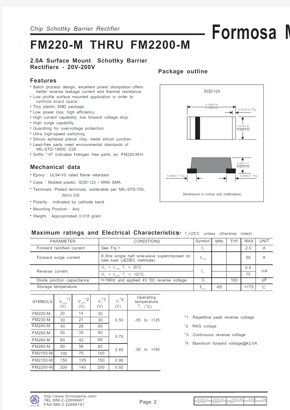
? Package outline
2.0A Surface Mount Schottky Barrier Rectifiers - 20V-200V PARAMETER
CONDITIONS Forward rectified current Forward surge current Reverse current
Diode junction capacitance Storage temperature
See Fig.1
8.3ms single half sine-wave superimposed on rate load (JEDEC methode)f=1MHz and applied 4V DC reverse voltage
Symbol
MIN.TYP.MAX.UNIT I O I FSM I R C J T STG
A A mA O
C
pF
2.0500.5+175
-65
FM220-M FM230-M FM240-M 203040142128203040-55 to +125
SYMBOLS V RRM (V)V RMS V R (V)(V)*1*2*3*1 Repetitive peak reverse voltage *2 RMS voltage
*3 Continuous reverse voltage *4 Maximum forward voltage@I =2.0A
F O V = V T = 25C R RRM J O V = V T = 100C
R RRM J 160
10
V F (V)
*4FM250-M FM260-M 5060354250600.700.50-55 to +150
FM280-M FM2100-M 0.8580100801005670O (C) Operating temperature T ,J FM2150-M 150150105FM2200-M
200
200
140
0.920.90Maximum ratings and Electrical Characteristics (AT T =25A
o
C unless otherwise noted)
Pinning information
Marking
Type number Marking code FM220-M 22FM230-M 23FM240-M 24FM250-M 25 FM260-M 26FM280-M 28 FM2100-M 20FM2150-M 215FM2200-M 220
Suggested solder pad layout
Dimensions in inches and (millimeters)
C
B 0.055 (1.40)
A 0.075 (1.90)
C 0.075 (1.90)
PACKAGE SOD-123
Packing information
Item
Tolerance SOD-123
Carrier width Carrier length Carrier depth Sprocket hole
13" Reel outside diameter 7" Reel outside diameter 13" Reel inner diameter 7" Reel inner diameter Feed hole diameter Sprocket hole position Punch hole position Punch hole pitch Sprocket hole pitch Embossment center Reel width
Overall tape thickness Tape width P 0P 1E B C d F T W P A D D D 1D 1D 2W 1
Symbol 0.10.10.1min min 0.50.10.31.0
0.10.10.10.10.10.12.02.0unit:mm
1.50
-178.00-62.0013.001.753.504.004.002.000.238.0011.40
D Note:Devices are packed in accor dance with EIA standar RS-481-A and specifications listed above.
1.903.901.68
Reel packing
SOD-1237"
2,500
4.0
25,000
183*183*123
178
382*262*387
200,000
9.5
PACKAGE
REEL SIZE
REEL COMPONENT SPACING
BOX INNER BOX REEL DIA,CARTON SIZE CARTON APPROX.GROSS WEIGHT
(kg)(pcs)(m/m)(m/m)(m/m)(pcs)(m/m)(pcs) Profile Feature Soldering Condition
Average ramp-up rate(T L to T P ) <3/sec
Preheat
o -Temperature Min(Tsmin) 150C o -Temperature Max(Tsmax) 200C -Time(min to max)(t s ) 60~120sec Tsmax to T L
o -Ramp-upRate <3C/sec Time maintained above:
o -Temperature(T L ) 217C -Time(t L ) 60~260sec o o Peak Temperature(T P ) 255C-0/+5C o Time within 5C of actual Peak Temperature(t P )
o Ramp-down Rate <6C/sec o Time 25C to Peak Temperature <6minutes
o
C
10~30sec
1.Storage environment: Temperature=5~40 Humidity=55%±25%o o C C Suggested thermal profiles for soldering processes
25
TL
TP
T e m p e r a t u r e
High reliability test capabilities
1. Solder Resistance
2. Solderability
3. High Temperature Reverse Bias
4. Forward Operation Life
5. Intermittent Operation Life
6. Pressure Cooker
7. Temperature Cycling
8. Thermal Shock
9. Forward Surge
10. Humidity
11. High Temperature Storage Life at 2605 for 102sec.
immerse body into solder 1/16"±1/32"
O
at 245±5C for 5 sec.
O
V=80% rate at T=125C for 168 hrs.
R J
O
Rated average rectifier current at T=25C for 500hrs.
A
O
T = 25C, I = I
A F O
On state: power on for 5 min.
off state: power off for 5 min.
on and off for 500 cycles.
O
15P at T=121C for 4 hrs.
SIG A
O O
-55C to +125C dwelled for 30 min.
and transferred for 5min. total 10 cycles.
O O
0C for 5 min. rise to 100C for 5 min. total 10 cycles.
8.3ms single half sine-wave superimposed
on rated load, one surge.
O
at T=85C, RH=85% for 1000hrs.
A
O
at 175C for 1000 hrs.
O
±C±MIL-STD-750D
METHOD-2031
MIL-STD-202F
METHOD-208
MIL-STD-750D
METHOD-1038
MIL-STD-750D
METHOD-1027
MIL-STD-750D
METHOD-1036
JESD22-A102
MIL-STD-750D
METHOD-1051
MIL-STD-750D
METHOD-1056
MIL-STD-750D
METHOD-4066-2
MIL-STD-750D
METHOD-1021
MIL-STD-750D
METHOD-1031
Item Test Conditions Reference