H.265 Encoder Board User Manual

MS3516A
H.265Encoder System User’s Manual
MS3516A H.265Encoder System
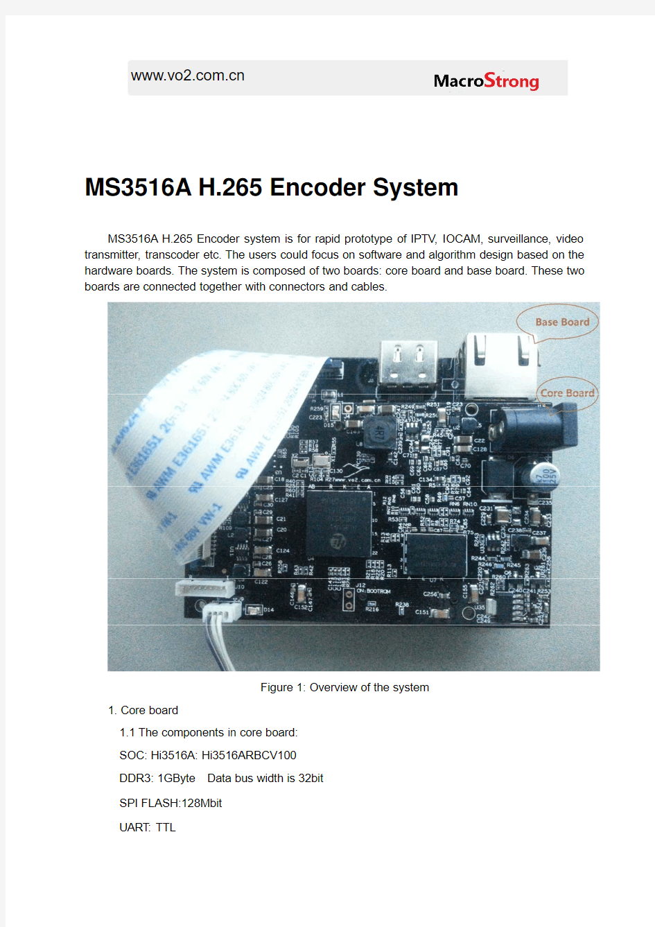
MS3516A H.265Encoder system is for rapid prototype of IPTV,IOCAM,surveillance,video transmitter,transcoder etc.The users could focus on software and algorithm design based on the hardware boards.The system is composed of two boards:core board and base board.These two boards are connected together with connectors and cables.
Figure1:Overview of the system
1.Core board
1.1The components in core board:
SOC:Hi3516A:Hi3516ARBCV100
DDR3:1GByte Data bus width is32bit
SPI FLASH:128Mbit
UART:TTL
SD CARD:MicroSD Socket
VIDEO INPUT CONNECTOR:
?8-/10-/12-/14-bit RGB Bayer CMOS sensor interface
?BT.601,BT.656,or BT.1120VI interface
THREE PERIPHERAL EXTENSION CONNECTOR
Core Board SIZE:51mm X84mm
Figure2Core Board Block diagram
1.2Connectors pinout
J15:DC12V power jack.9V~14V DC power supply input connector
1-+12V2-GND3-GND
J1:40-way Video input connector.Could be connected to the Video output connectors via a FPC cable as Figure1.The pin map is indicated in Figure2.
J10:JTAG connector.Could be connected to ARM JTAG debugger adapter for software debugging.
1,2-DC3.3V power output
3-RESETn
4-TDI
5-TMS
6-TCK
7-TDO
8-GND
J9:UART0with TTL level.Could be connected to the PC’s UART port via a TTL-RS232level translator,or connected to PC’s USB port via USB-TTL UART adapter.The UART0is used as software debug port,always we use it as the terminal of LINUX.
1-DC 3.3V power output
2-UART0-RXD(input)
3-UART0-TXD(output)
4-GND
J4:Test point ,wired to GND
J1pin #Signal Name J1pin #Signal Name 1GPIO 2DC12V power output 3GND
4GND 5DC5V power output 6GND 7VI_DATA78VI_DATA69VI_DATA510VI_DATA411VI_DATA312VI_DATA213VI_DATA114VI_DATA015VI_HSYNC 16VI_PIXEL CLK 17VI_VSYNC 18GND
19SENSORCLK 20SPI_CLK/I2C_SCL 21SPI_CSn 22SPI_MISO 23NC 24GPIO 25GND 26GND 27GND
28NC 29SPI_MOSI_I2C_SDA 30VI_DATA1531VI_DATA1432VI_DATA1333VI_DATA1234VI_DATA1135VI_DATA1036VI_DATA937VI_DATA838GPIO 39
GPIO
40
GND
J12:Jumper.Boot mode selector.Should be shorted if you want to erase or reprogram the uboot code in the FLASH.
J13(Located on bottom side):Peripheral extension,including SPI,I2C,SDIO,GPIO
J13pin#Signal Name J13pin#Signal Name
1Power on reset output40GND
2GPIO39SPI1_CLK/I2C1_SCL
3GPIO38SPI1_CSn
4GPIO37SPI1_MOSI
5GPIO36SPI1_MISo
6GPIO35SDIO1_CMD
7GPIO34SDIO1_CARD_DETECT
8GPIO33SDIO1_DATA2
9GPIO32SDIO1_DATA0
10GPIO31SDIO1_DATA3
11GPIO30DC5V output
12GPIO29SDIO1_CLKOUT
13GPIO28GPIO
14GPIO27GPIO
15GPIO26GPIO
16SDIO1_POWER_EN25GPIO
17SDIO1_DATA124GPIO
18GPIO23GPIO
19GND22GPIO
20GND21GND
J2(Located on bottom side):Peripheral extension,including video output and ethernet phy
J2pin#Signal Name J2pin#Signal Name
1Power on reset output40GND
2RGMII_RXD339RGMII_RXD0
J3(Located on bottom side):Peripheral extension,including analog audio in/out,analog video output,USB,I2C,UART
3RGMII_RX_CLK 38RGMII_RXD24RGMII_TXD037MDCLK 5RGMII_TXD236RGMII_RX_DV
6RGMII_TX_CLK 35Reset Eth PHY(active low)7RGMII_TXD134MDIO
8VideoOut_DATA1533VideoOut_DATA109VideoOut_DATA1332VideoOut_DATA1410VideoOut_DATA1131VideoOut_DATA1211DC5V output 30DC5V output 12VideoOut_DATA129VideoOut_DATA613VideoOut_DATA228RGMII_RXD114VideoOut_PIXELCLK 27RGMII_TX_EN 15NC
26RGMII_TXD316VideoOut_DATA725ETH PHY CLK 17VideoOut_DATA524VideoOut_DATA318VideoOut_DATA423VideoOut_DATA919VideoOut_DATA022VideoOut_DATA820
GND
21
GND
J2pin #Signal Name
J2pin #Signal Name 1Power on reset output 40GND 2Audio Analog input 39USB_DM 3Audio Analog input 38USB_DP 4NC 37GPIO 5NC 36NC
6
NC
35
Audio Analog(DC bias)
7NC34Audio Analog output
8NC33Audio Analog output
9NC32I2C2_SDA
10UART1_TXD31UART2_TXD
11DC5V output30DC5V output
12UART1_RXD29I2S_MCLK
13GPIO28I2S_SD_RX
14I2C2_SCL27CVBS Video Analog
output
15NC26GPIO
16GPIO25UART2_RXD
17GPIO24I2S_BCLK_TX
18NC23I2S_SD_TX
19NC22I2S_WS_TX
20GND21GND
Figure3Core Board layout
2.Base board
The base board could be stacked under the core board for peripheral extension.Also a 40-way FPC cable should be plugged between the core board and base board.
2.1The components in base board:
ADV7619:HDMI receiver,convert HDMI1.4a to BT1120interface
SII9022:HDMI transmitter,convert BT1120to HDMI1.4a
RTL8211E:10/100/1000M ethernet transceiver
UART:TTL interface
USB:in the form of a mini-pcie socket or type-a USB connector
Video Output Connector:BT.1120interface,connected to the core board via a40-way FPC cable
Two peripheral connectors:stack under the core board
Base Board SIZE:66mm X84mm
Figure4:Base Board layout
2.2Functions
2.2.1HDMI receiver
The HDMI video source should be connected at the J5HDMI socket,which is wired to the HDMI1port of ADV7619.
The I2C address is0x98.
The video output port is connected to Hi3516A’s MIPI/VI_DATA port.The
OP_FORMAT_SEL[7:0]should be set to0x80(16bit SDR ITU-R BT.656Mode0)to conform Hi3516A’s BT1120timing requirements
The I2S port is connected to Hi3516A’s I2S port(Group of pin#Y7,Y5,W5,W6)
Signal Name ADV7619PIN Hi3516A pin#Discription
VI_DATA0P4(pin#87)AB10Cr0,Cb0
VI_DATA1P5(pin#86)AA10Cr0,Cb0
VI_DATA2P6(pin#85)W9Cr0,Cb0
VI_DATA3P7(pin#84)Y9Cr0,Cb0
VI_DATA4P8(pin#83)Y10Cr0,Cb0
VI_DATA5P9(pin#82)W10Cr0,Cb0
VI_DATA6P10(pin#81)AB11Cr0,Cb0
VI_DATA7P11(pin#80)AA11Cr0,Cb0
VI_DATA8P16(pin#73)AB12Y0
VI_DATA9P17(pin#72)AA12Y1
VI_DATA10P18(pin#71)W12Y2
VI_DATA11P19(pin#70)Y12Y3
VI_DATA12P20(pin#69)Y13Y4
VI_DATA13P21(pin#68)W13Y5
VI_DATA14P22(pin#67)AB13Y6
VI_DATA15P23(pin#66)AA13Y7
VI_PIXEL CLK LLC((pin#62)AB14PIXEL CLOCK
2.2.2HDMI transmitter
An SII9022HDMI transmitter would translate the Hi3516A’s BT1120video output to HDMI.J2is the HDMI output socket.
Ci2CA is pulled low,so the I2C address should be:
Transmitter Programming Interface(TPI)device address0x72
CEC Programming Interface(CPI)device address0xC0
SiI9020-compatible internal registers:first device address0x72
SiI9020-compatible internal registers:second device address0x7A
The video input port is connected to Hi3516A’s VO port.The output mode should be set to16-Bit YC4:2:2Embedded Sync mode to conform Hi3516A’s BT1120timing requirements
The I2S port is left open,so audio output is not supported here.
2.2.3USB
The USB port of Hi3516A is connected to both the MiniPCIe socket and a USB Type A socket.So MiniPCIe and USB Type A socket could not be used at the same time.Normally a4G module has a MiniPCIe interface,a WIFI module has a USB interface.
To use4G module,a MiroSIM card should be plugged in the J4socket.
In case multiple USB devices needed,maybe a external USB HUB could be connected to the USB port.
2.2.4UART
Except for the J9socket in core board for UART0,there’s another TTL level UART in base board,it is connected to UART1of Hi3516A.
Web site:https://www.sodocs.net/doc/eb15866350.html,
Email:sales@https://www.sodocs.net/doc/eb15866350.html,