2.Five-Level Diode-Clamped Inverter With Three-Level Boost Converter
Five-Level Diode-Clamped Inverter With Three-Level Boost Converter Rosmadi Abdullah,Member,IEEE,Nasrudin Abd.Rahim,Senior Member,IEEE, Siti Rohani Sheikh Raihan,Member,IEEE,and Abu Zaharin Ahmad,Member,IEEE
Abstract—This paper proposes an active front-end solution to balance the dc-link capacitor voltage of the?ve-level diode-clamped inverter.Capacitor voltage balancing is performed by a three-level boost converter connected to the two inner capacitors of a?ve-level diode-clamped inverter and additional balancing circuits at the other two outer capacitors.The proposed con?g-uration is tested through simulation and experiment for various load power factor conditions at a high modulation index.The result demonstrates the reliability of the proposed con?guration to balance the dc-link capacitor voltage at the desired level.
Index Terms—DC-link capacitor voltage balancing,diode-clamped,multilevel inverter,three-level boost converter(TLBC).
I.I NTRODUCTION
T HREE highly popular voltage-source multilevel inverters can be divided into three categories according to their topology:neutral point clamped,?ying capacitor,and cascade H-bridge[1]–[3],[40],[41].Studies on three-,four-,?ve-and six-level diode-clamped inverters for such use like static V AR compensators,high voltage grid interconnections,and variable speed motor drives have been considered[4]–[16].It has long been recognized that,for the diode-clamped inverter with more than three levels,a passive front-end capacitor voltage balanc-ing method is only achievable if the modulation index is limited to about60%of its maximum value for loads with a typical 0.8power factor[17]–[20].If the modulation index is increased more than this value,the center capacitors gradually discharge, and?nally,the inverter output converges at three levels[21].To overcome this limitation,a multilevel inverter can be supplied by isolated dc sources[16],[22]such as external circuit as the active front-end solution of dc-link capacitor balancing [17],[21],[23]–[26],using balancing circuit by transferring charge from one capacitor to another capacitor to equilibrium level[11],[12],[27]or the modi?cation of the pulsewidth
Manuscript received August19,2013;revised November4,2013;accepted November29,2013.Date of publication January2,2014;date of current version May2,2014.
R.Abdullah is with the Department of Electrical Engineering,University of Malaya,Kuala Lumpur50603,Malaysia,and also with the Faculty of Electrical and Electronics Engineering,Universiti Malaysia Pahang,Pahang 26300,Malaysia(e-mail:rosmadi@https://www.sodocs.net/doc/fd4960304.html,.my).
N. A.Rahim and S.R.Sheikh Raihan are with the University of Malaya Power Energy Dedicated Centre(UMPEDAC),University of Malaya, Kuala Lumpur59990,Malaysia(e-mail:nasrudin@https://www.sodocs.net/doc/fd4960304.html,.my;srohani_sr@ https://www.sodocs.net/doc/fd4960304.html,.my).
A.Z.Ahmad is with the Faculty of Electrical and Electronics Engineer-ing,Universiti Malaysia Pahang,Pahang26600,Malaysia(e-mail:zaharin@ https://www.sodocs.net/doc/fd4960304.html,.my).
Color versions of one or more of the?gures in this paper are available online at https://www.sodocs.net/doc/fd4960304.html,.
Digital Object Identi?er
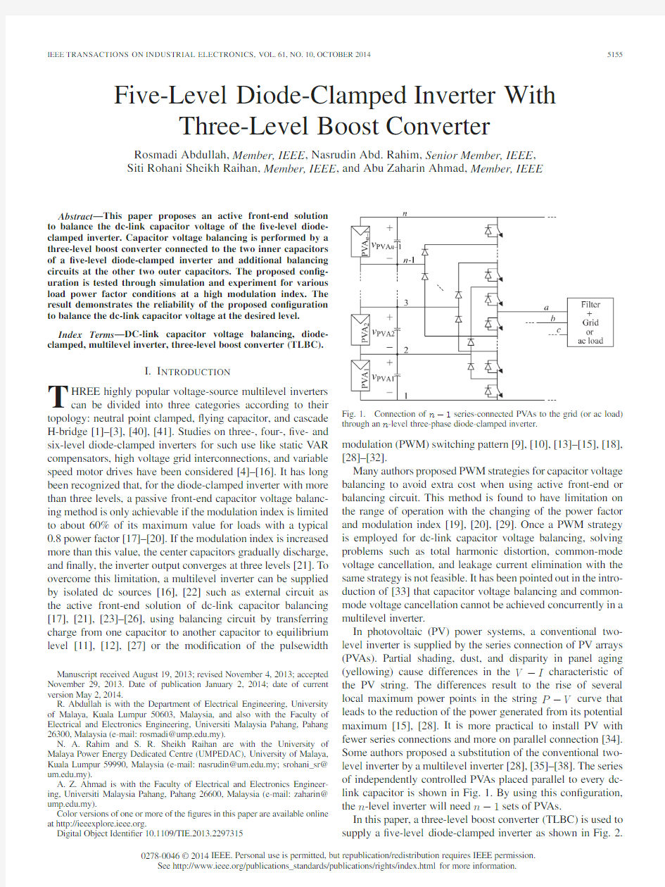
10.1109/TIE.2013.2297315Fig.1.Connection of n?1series-connected PV As to the grid(or ac load) through an n-level three-phase diode-clamped inverter.
modulation(PWM)switching pattern[9],[10],[13]–[15],[18], [28]–[32].
Many authors proposed PWM strategies for capacitor voltage balancing to avoid extra cost when using active front-end or balancing circuit.This method is found to have limitation on the range of operation with the changing of the power factor and modulation index[19],[20],[29].Once a PWM strategy is employed for dc-link capacitor voltage balancing,solving problems such as total harmonic distortion,common-mode voltage cancellation,and leakage current elimination with the same strategy is not feasible.It has been pointed out in the intro-duction of[33]that capacitor voltage balancing and common-mode voltage cancellation cannot be achieved concurrently in a multilevel inverter.
In photovoltaic(PV)power systems,a conventional two-level inverter is supplied by the series connection of PV arrays (PV As).Partial shading,dust,and disparity in panel aging (yellowing)cause differences in the V?I characteristic of the PV string.The differences result to the rise of several local maximum power points in the string P?V curve that leads to the reduction of the power generated from its potential maximum[15],[28].It is more practical to install PV with fewer series connections and more on parallel connection[34]. Some authors proposed a substitution of the conventional two-level inverter by a multilevel inverter[28],[35]–[38].The series of independently controlled PV As placed parallel to every dc-link capacitor is shown in Fig.1.By using this con?guration, the n-level inverter will need n?1sets of PV As.
In this paper,a three-level boost converter(TLBC)is used to supply a?ve-level diode-clamped inverter as shown in Fig.2.
0278-0046?2014IEEE.Personal use is permitted,but republication/redistribution requires IEEE permission.
See https://www.sodocs.net/doc/fd4960304.html,/publications_standards/publications/rights/index.html for more information.
Fig.2.Proposed three-level (TL)boost chopper and balancer circuit for C1and
C4.
Fig.3.Switching signal and inductance current waves of boost TL chopper.
In energy conversion system,a boost chopper is often used due to its simple topology and control method [23]–[25],[39].The TLBC has advantages in high power applications such as reduced switching losses and reduced reverse recovery losses of the diode [23].With reduced inductor current ripple in TLBC,a smaller size inductor can be used in TLBC compared to the conventional boost converter [26].
DC-link capacitor voltage balancing is performed using a combination of active front-end and balancing circuits.TLBC is used to balance the two inner capacitors,C1and C2,and another balancing circuit is used to balance the outer capacitors,C1and C4,by transferring the charge from the inner capacitors to the outer capacitors.All control functions for TLBC,balanc-ing circuits,and the ?ve-level inverter are implemented fully in software with a Texas Instruments TMS320F28335digital signal controller (DSC).Laboratory experiment results are ob-tained from a 1.1-kW prototype.The proposed con?guration is suitable for a grid-connected PV system which operates in unidirectional power ?ow.The prototype is tested for various load power factor conditions to evaluate its performance at a high modulation index.
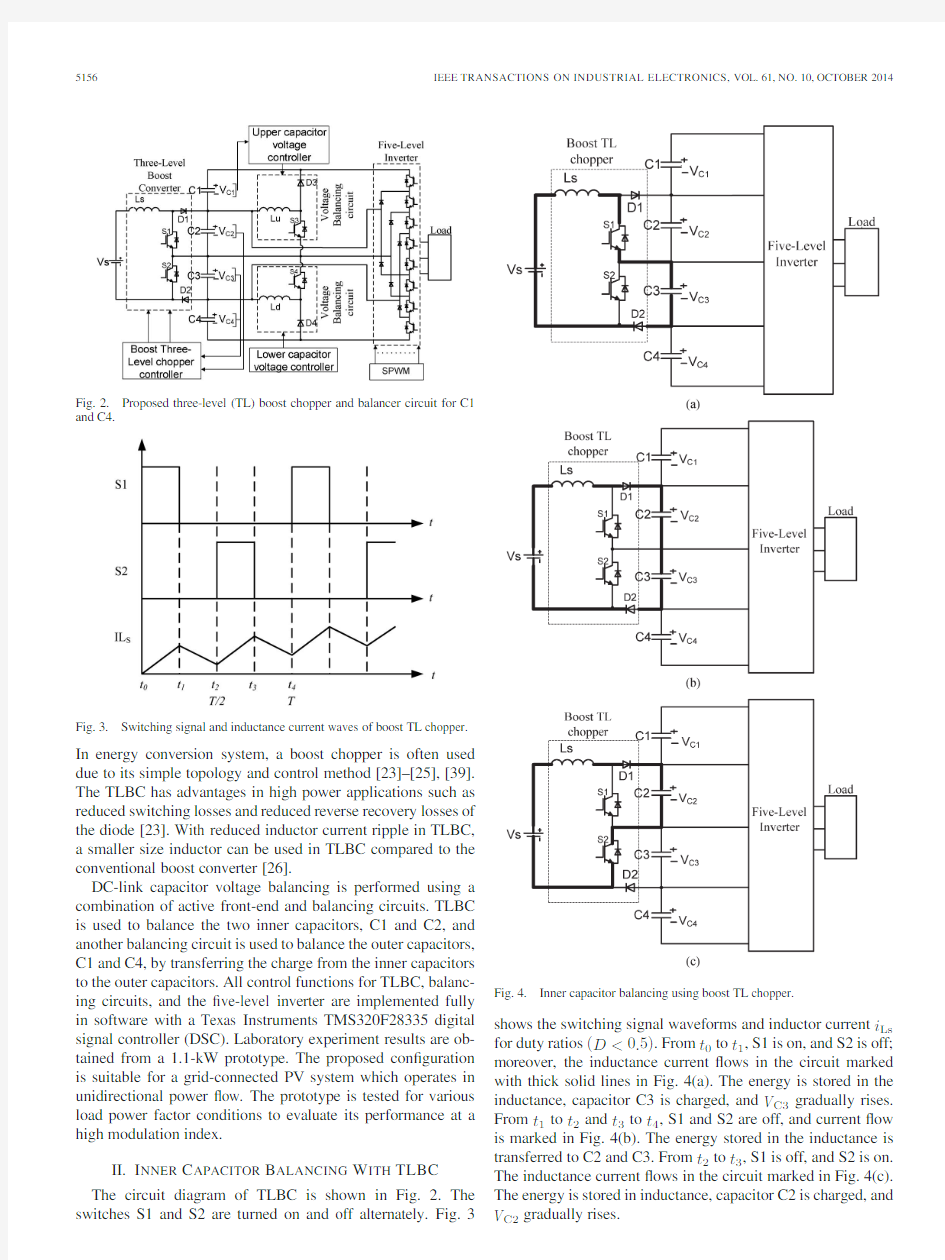
II.I NNER C APACITOR B ALANCING W ITH TLBC The circuit diagram of TLBC is shown in Fig. 2.The switches S1and S2are turned on and off alternately.Fig.
3
Fig.4.Inner capacitor balancing using boost TL chopper.
shows the switching signal waveforms and inductor current i Ls for duty ratios (D <0.5).From t 0to t 1,S1is on,and S2is off;moreover,the inductance current ?ows in the circuit marked with thick solid lines in Fig.4(a).The energy is stored in the inductance,capacitor C3is charged,and V C3gradually rises.From t 1to t 2and t 3to t 4,S1and S2are off,and current ?ow is marked in Fig.4(b).The energy stored in the inductance is transferred to C2and C3.From t 2to t 3,S1is off,and S2is on.The inductance current ?ows in the circuit marked in Fig.4(c).The energy is stored in inductance,capacitor C2is charged,and V C2gradually rises.
ABDULLAH et al.:FIVE-LEVEL DIODE-CLAMPED INVERTER WITH THREE-LEVEL BOOST CONVERTER
5157
Fig.5.Control diagram of the boost TL chopper.
Capacitors C2and C3can be charged differently to the de-sired voltage level by controlling the duty ratios D.Increasing the time duration from t0to t1will increase the voltage at capacitor C3,and increasing the time duration from t2to t3 will increase the voltage at capacitor C2.
TLBC can be operated in?ve different algorithms[26].In this paper,only one algorithm where the time switching of S1 and that of S2do not overlapped each other is used.
The boost feature of the TLBC can be written as
V o=V C2+V C2=
2V s
(2?D)
(1)
where D is the duty ratio of this algorithm(2t1/T).D is varied from0to1.
The current ripple for the conventional boost inverter can be written as
ΔI=V s DT sw/L s(2) where T sw is the switching frequency of the conventional boost converter.
The current ripple for TLBC operation is
ΔI=V o(1?V s/V o)(2V s/V o?1)
2L s f sw
(3)
where f sw is the switching frequency of the conventional boost converter.
From(2)and(3),it shows that the current ripple of TLBC is half of the ripple produced by the conventional boost converter. It suggests that an inductor of smaller size can be used in the TLBC.
To ensure the equal voltage of capacitors C2and C3,a voltage balancing controller for TLBC,shown in Fig.5,is used. The duty ratio of the boost switches S1and S2is controlled by using a proportional-integral-derivative(PID)controller where V ref is the desired dc voltage at C2and C3.The PID controller for voltage regulation is designed to have a proportional gain (Kp)of20,an integral gain(Ki)of0.003,and a derivative gain (Kd)of10.
Normally,by using a passive method[11],[12],the dc source is connected between outer capacitors C1and C4as shown in Fig.2,which is four times the individual capacitor voltage level. More series strings of PV panels need to be used to provide higher voltage which is impractical in PV installation[34].
The Fig.6.Outer capacitor balancing
circuit.
Fig.7.Balancing circuit control
diagram.
Fig.8.DC-link capacitor voltage balancing using PID controller. proposed con?guration requires lower voltage level as shown in Fig.4,where the outer capacitors are not supplied directly from the TLBC.This method is more practical since only one set of PV As with fewer series-connected PV panels is used.
5158IEEE TRANSACTIONS ON INDUSTRIAL ELECTRONICS,VOL.61,NO.10,OCTOBER
2014
Fig.9.Simulation results.High resistive load(power factor(PF)=0.999).(a)DC-link voltage and inductor current.(b)Inverter output phase voltage,line–line output voltage,and output line current.
III.O UTER C APACITOR B ALANCING
Outer capacitors C1and C4are controlled by using the balancing circuit shown in Fig.6.The voltage at C1,V c1,is charged to the voltage level equal to V c2,and the voltage at C4, V c4,is charged to the voltage level equal to V c3by adjusting the duty ratio of S3and S4,respectively.Fig.7shows the PID controllers used to balance the upper capacitor C1and lower capacitor C4.
The controller is designed with the value Kp=10,Ki= 0.001,and Kd=10.Increasing the duty ratio of S3and S4 will reduce the charging time of V C1and V C4,respectively. However,if the duty ratio is too high,the middle capacitors C2and C3will overdischarge and reduce the voltage at these capacitors.To solve this problem,the controller in Fig.7must operate at a slower rate than the TLBC controller shown in Fig.5.Fig.8shows the simulation result performance of both the PID controllers balancing all four dc-link capacitors. During steady state,the upper inductor and lower induc-tor currents?ow continuously(ILu(t)>0and ILd(t)>0). Therefore,the time integral of the inductor voltage over one time period must be zero
V C2t3on+V C1t3o?=0.(4) If V C2and V C1are equal in magnitude,the steady-state duty cycle of switch S3will be0.5.The duty cycle for switch S4will also be0.5if V C3is equal to V C4.
IV.S IMULATION R ESULTS
The proposed con?guration has been simulated using MATLAB/Simulink for the BLTC connected to a?ve-level diode-clamped inverter.The switching frequency of the BLTC was5kHz.To examine the balancing of dc-link capacitor volt-age,a?ve-level diode-clamped inverter with a high modulation index of1.0is connected to variations of the load power factor. The results,including dc-link capacitor voltages,inductor current(I Ls),inverter load voltages,and inverter load current, are shown in Fig.9.The magnitude of the reference load voltage is200Vrms,the magnitude of the reference dc-link capacitor voltage is82V,and the RL load is150Ωand 28.7mH.The frequency of the load voltage is50Hz,and the power factor of the load is0.99.Fig.9(a)shows the dc-link voltage of82V and the BLTC inductor current of3.2A.The dc-link voltages have been regulated with small errors,and the performance of the?ve-level inverter is shown in Fig.9(b). The performance of the system is examined for lower power factor and higher frequency.The inverter reference frequency is increased to100Hz,and the load power factor is reduced to0.95with the RL load of54.7Ωand28.7mH.The dc-link capacitor voltage,load output voltage,and load current are illustrated in Fig.10.
To examine with more inductive load,the load resistance is decreased to24Ω.Therefore,the power factor has decreased to 0.8,and the dc-link capacitor voltage,load output voltage,and load current are presented in Fig.11.It can be observed from
ABDULLAH et al.:FIVE-LEVEL DIODE-CLAMPED INVERTER WITH THREE-LEVEL BOOST CONVERTER5159
Fig.10.Simulation results.Low inductive load(power factor(PF)=0.95).(a)DC-link voltage and inductor current.(b)Inverter output phase voltage,line–line output voltage,and output line current.
Fig.11.Simulation results.Highly inductive load(power factor(PF)=0.8).(a)DC-link voltage and inductor current.(b)Inverter output phase voltage, line–line output voltage,and output line current.
5160IEEE TRANSACTIONS ON INDUSTRIAL ELECTRONICS,VOL.61,NO.10,OCTOBER 2014
TABLE I
P ARAMETERS OF THE E XPERIMENTAL C IRCUIT IN F IG .
1
Fig.12.Capacitor voltages V C1,V C2,V C3,and V C4when TLBC controller operated and both inner capacitor controller and outer capacitor controller operated.
Figs.9–11that the dc-link voltage balancing performs well at a high modulation index and various power factor conditions.The inverter performance also has not been affected by the power factor change.
V .E XPERIMENTAL R ESULTS
For the veri?cation of the simulation results,the labora-tory experiment setup shown in Fig.1has been developed and tested.The controllers for the boost three-level converter and inverter have been developed on a Texas Instruments TMS320F28335DSC.The parameters of the system are shown in Table I.
Fig.12presents the voltage waveforms measured at the capacitors C1,C2,C3,and C4.To examine the response of the system,initially,the TLBC controller is operated to regulate the inner capacitor voltage to the desired target value of 40V ,whereas the outer capacitor voltage controller is turned off.Then,the outer capacitor voltage controller is turned on,and the outer capacitor voltage is increased to 40V .When all dc-link capacitors’voltages exceed 40V ,a new capacitor value V ref of 60V is set.It can be observed that the dc-link
capacitor
Fig.13.Experimental results.High power factor (0.99).(a)Inductor current (I Ls ),load voltage (V aM and V ab ),and load current (I a ).(b)Capacitor voltages V C1,V C2,V C3,and V C4at 82V .
voltage controller operates satisfactorily when regulating all of the dc-link capacitors to the new reference value of 60V .
To validate the performance of the system with a high modulation index regardless of changing the load power factor,three experiments have been conducted and evaluated.Fig.13shows the experiment results when the inverter is supplying a highly resistive load (power factor of 0.9).The frequency of the inverter reference is 50Hz,and the RL load of the inverter is 150Ωand 28.7mH.It can be observed that the dc-link capacitor voltage regulates at 82V with small errors and the ?ve-level diode-clamped inverter operates satisfactorily.
To examine the performance of the system for higher fre-quency and lower power factor,the inverter reference frequency is increased to 100Hz,and the resistor load is decreased to 54.7Ω.Therefore,the load power factor decreases to 0.95.The TLBC inductor current,load voltage,and load current are illustrated in Fig.14(a).DC-link voltages are shown in Fig.14(b).
To examine a more inductive load,the resistive load is decreased to 20Ω;therefore,the power factor has decreased to 0.8.The TLBC inductor current,load voltage,and load current are illustrated in Fig.15(a),and dc-link voltages are shown in Fig.15(b).
ABDULLAH et al.:FIVE-LEVEL DIODE-CLAMPED INVERTER WITH THREE-LEVEL BOOST CONVERTER
5161
Fig.14.Experimental results.Low inductive load(power factor=0.95).
(a)Inductor current(I Ls),load voltage(V aM and V ab),and load current(I a).
(b)Capacitor voltages V C1,V C2,V C3,and V C4at82V.
It can be seen from Figs.13–15that the dc-link capacitor balancing performance is not affected by the changing of the load power factor,even though the inverter has operated at a high modulation index.
VI.C ONCLUSION
This paper has proposed a new con?guration to balance the dc-link capacitor voltages of the?ve-level diode-clamped in-verter.Connecting a TLBC at the input of the inverter regulates the two inner dc-link capacitors’voltage at the desired level with the changing of the converter dc source and,at the same time,provides voltage balancing.Balancing circuits are added to balance the voltage of the two outer capacitors.
Overall,the investigations show that the proposed converter operates well in various load power factor conditions.This con?guration is suitable for the grid-connected PV system due to the unidirectional power transfer.In addition,only one set of PV As is needed instead of four sets of independently controlled PV As required to supply the inverter in the conventional
system.Fig.15.Experimental results.High inductive load(power factor=0.8).
(a)Inductor current(I Ls),load voltage(V aM and V ab),and load current(I a).
(b)Capacitor voltages V C1,V C2,V C3,and V C4at82V.
R EFERENCES
[1]A.Nabae,I.Takahashi,and H.Akagi,“A new neutral-point-clamped
PWM inverter,”IEEE Trans.Ind.Appl.,vol.IA-17,no.5,pp.518–523, Sep.1981.
[2]C.Hochgraf,https://www.sodocs.net/doc/fd4960304.html,sseter,D.Divan,and T.A.Lipo,“Comparison of
multilevel inverters for static V Ar compensation,”in Conf.Rec.IEEE IAS Annu.Meeting,1994,vol.2,pp.921–928.
[3]M.Marchesoni and M.Mazzucchelli,“Multilevel converters for high
power ac drives:A review,”in Proc.IEEE Int.Symp.Ind.Electron.,1993, pp.38–43.
[4]J.Rodriguez,S.Bernet,P.K.Steimer,and I.E.Lizama,“A survey
on neutral-point-clamped inverters,”IEEE Trans.Ind.Electron.,vol.57, no.7,pp.2219–2230,Jul.2010.
[5]B.A.Welchko,“A three-level MOSFET inverter for low-power drives,”
IEEE Trans.Ind.Electron.,vol.51,no.3,pp.669–674,Jun.2004. [6]A.Bendre,S.Krstic,J.Vander Meer,and G.Venkataramanan,“Com-
parative evaluation of modulation algorithms for neutral-point-clamped converters,”IEEE Trans.Ind.Appl.,vol.41,no.2,pp.634–643, Mar./Apr.2005.
[7]N.Hatti,Y.Kondo,and H.Akagi,“Five-level diode-clamped PWM con-
verters connected back-to-back for motor drives,”IEEE Trans.Ind.Appl., vol.44,no.4,pp.1268–1276,Jul./Aug.2008.
[8]N.Hatti,K.Hasegawa,and H.Akagi,“A6.6-kV transformerless motor
drive using a?ve-level diode-clamped PWM inverter for energy savings
5162IEEE TRANSACTIONS ON INDUSTRIAL ELECTRONICS,VOL.61,NO.10,OCTOBER2014
of pumps and blowers,”IEEE Trans.Power Electron.,vol.24,no.3, pp.796–803,Mar.2009.
[9]M.M.Renge and H.M.Suryawanshi,“Five-level diode clamped inverter
to eliminate common mode voltage and reduce dv/dt in medium voltage rating induction motor drives,”IEEE Trans.Power Electron.,vol.23, no.4,pp.1598–1607,Jul.2008.
[10]M.M.Renge and H.M.Suryawanshi,“Three-dimensional space-vector
modulation to reduce common-mode voltage for multilevel inverter,”
IEEE Trans.Ind.Electron.,vol.57,no.7,pp.2324–2331,Jul.2010. [11]K.Hasegawa and H.Akagi,“Low-modulation-index operation of a?ve-
level diode-clamped PWM inverter with a dc-voltage-balancing circuit for
a motor drive,”IEEE Trans.Power Electron.,vol.27,no.8,pp.3495–
3504,Aug.2012.
[12]K.Hasegawa and H.Akagi,“A new dc-voltage-balancing circuit
including a single coupled inductor for a?ve-level diode-clamped PWM inverter,”IEEE Trans.Ind.Appl.,vol.47,no.2,pp.841–852, Mar./Apr.2011.
[13]H.A.Hotait,A.M.Massoud,S.J.Finney,and B.W.Williams,“Capacitor
voltage balancing using redundant states of space vector modulation for ?ve-level diode clamped inverters,”IET Power Electron.,vol.3,no.2, pp.292–313,Mar.2010.
[14]M.Saeedifard,R.Iravani,and J.Pou,“Control and dc-capacitor voltage
balancing of a space vector-modulated?ve-level STATCOM,”IET Power Electron.,vol.2,no.3,pp.203–215,May2009.
[15]S.Busquets-Monge,J.Rocabert,P.Rodriguez,S.Alepuz,and
J.Bordonau,“Multilevel diode-clamped converter for photovoltaic gen-erators with independent voltage control of each solar array,”IEEE Trans.
Ind.Electron.,vol.55,no.7,pp.2713–2723,Jul.2008.
[16]E.Ozdemir,S.Ozdemir,and L.M.Tolbert,“Fundamental-frequency-
modulated six-level diode-clamped multilevel inverter for three-phase stand-alone photovoltaic system,”IEEE Trans.Ind.Electron.,vol.56, no.11,pp.4407–4415,Nov.2009.
[17]A.A.Boora,A.Nami,F.Zare,A.Ghosh,and F.Blaabjerg,“V oltage-
sharing converter to supply single-phase asymmetrical four-level diode-clamped inverter with high power factor loads,”IEEE Trans.Power Electron.,vol.25,no.10,pp.2507–2520,Oct.2010.
[18]M.Fracchia,T.Ghiara,M.Marchesoni,and M.Mazzucchelli,“Opti-
mized modulation techniques for the generalized N-level converter,”in Proc.23rd IEEE PESC,1992,vol.2,pp.1205–1213.
[19]M.Saeedifard,R.Iravani,and J.Pou,“Analysis and control of dc-
capacitor-voltage-drift phenomenon of a passive front-end?ve-level con-verter,”IEEE Trans.Ind.Electron.,vol.54,no.6,pp.3255–3266,Dec.2007.
[20]M.Saeedifard,R.Iravani,and P.Josep,“A space vector modulation strat-
egy for a back-to-back?ve-level HVDC converter system,”IEEE Trans.
Ind.Electron.,vol.56,no.2,pp.452–466,Feb.2009.
[21]P.Fang Zheng,L.Jih-Sheng,J.McKeever,and J.VanCoevering,“A
multilevel voltage-source converter system with balanced dc voltages,”in Proc.26th IEEE PESC,1995,vol.2,pp.1144–1150.
[22]R.W.Menzies,P.Steimer,and J.K.Steinke,“Five-level GTO inverters
for large induction motor drives,”IEEE Trans.Ind.Appl.,vol.30,no.4, pp.938–944,Jul./Aug.1994.
[23]K.Jung-Min,K.Bong-Hwan,and N.Kwang-Hee,“Three-phase pho-
tovoltaic system with three-level boosting MPPT control,”IEEE Trans.
Power Electron.,vol.23,no.5,pp.2319–2327,Sep.2008.
[24]M.Malinowski,W.Kolomyjski,M.P.Kazmierkowski,and S.Stynski,
“Control of variable-speed type wind turbines using direct power control space vector modulated3-level PWM converter,”in Proc.IEEE Int.Conf.
Ind.Technol.,2006,pp.1516–1521.
[25]M.Hengchun,D.Boroyevich,and F.C.Lee,“Multi-level2-quadrant
boost choppers for superconducting magnetic energy storage,”in Proc.
Appl.Power Electron.Conf.Expo.,1996,vol.2,pp.876–882.
[26]V.I.Meleshin,D.V.Zhiklenkov,and A.A.Ganshin,“Ef?cient three-level
boost converter for various applications,”in Proc.Power Electron.Motion Control Conf.,2012,pp.DS1e.9-1–DS1e.9-8.
[27]C.Newton,M.Sumner,and T.Alexander,“The investigation and devel-
opment of a multi-level voltage source inverter,”in Proc.6th Int.Conf.
Power Electron.Variable Speed Drives,1996,pp.317–321.
[28]S.Alepuz,S.Busquets-Monge,J.Bordonau,J.Gago,D.Gonzalez,and
J.Balcells,“Interfacing renewable energy sources to the utility grid us-ing a three-level inverter,”IEEE Trans.Ind.Electron.,vol.53,no.5, pp.1504–1511,Oct.2006.
[29]S.A.Khajehoddin,A.Bakhshai,and P.K.Jain,“A simple voltage bal-
ancing scheme for m-level diode-clamped multilevel converters based on
a generalized current?ow model,”IEEE Trans.Power Electron.,vol.23,
no.5,pp.2248–2259,Sep.2008.
[30]S.Busquets-Monge,S.Alepuz,J.Bordonau,and J.Peracaula,“V oltage
balancing control of diode-clamped multilevel converters with passive
front-ends,”IEEE Trans.Power Electron.,vol.23,no.4,pp.1751–1758, Jul.2008.
[31]S.Busquets-Monge,J.Bordonau,and J.Rocabert,“A virtual-vector
pulsewidth modulation for the four-level diode-clamped dc-ac converter,”
IEEE Trans.Power Electron.,vol.23,no.4,pp.1964–1972,Jul.2008.
[32]S.Busquets-Monge,S.Alepuz,J.Rocabert,and J.Bordonau,“Pulsewidth
modulations for the comprehensive capacitor voltage balance of n-level three-leg diode-clamped converters,”IEEE Trans.Power Elec-tron.,vol.24,no.5,pp.1364–1375,May2009.
[33]A.V on Jouanne, D.Shaoan,and Z.Haoran,“A multilevel inverter
approach providing dc-link balancing,ride-through enhancement,and common-mode voltage elimination,”IEEE Trans.Ind.Electron.,vol.49, no.4,pp.739–745,Aug.2002.
[34]A.M?ki and S.Valkealahti,“Power losses in long string and parallel-
connected short strings of series-connected silicon-based photovoltaic modules due to partial shading conditions,”IEEE Trans.Energy Convers., vol.27,no.1,pp.173–183,Mar.2012.
[35]M.Calais and V.G.Agelidis,“Multilevel converters for single-phase grid
connected photovoltaic systems—An overview,”in Proc.IEEE Int.Symp.
Ind.Electron.,1998,vol.1,pp.224–229.
[36]K.Feel-Soon,P.Sung-Jun,C.Su Eog,U.K.Cheul,and T.Ise,“Multilevel
PWM inverters suitable for the use of stand-alone photovoltaic power systems,”IEEE Trans.Energy Convers.,vol.20,no.4,pp.906–915, Dec.2005.
[37]O.Alonso,P.Sanchis,E.Gubia,and L.Marroyo,“Cascaded H-bridge
multilevel converter for grid connected photovoltaic generators with in-dependent maximum power point tracking of each solar array,”in Proc.
34th IEEE PESC,2003,vol.2,pp.731–735.
[38]H.Ertl,J.W.Kolar,and F.C.Zach,“A novel multicell dc-ac converter for
applications in renewable energy systems,”IEEE Trans.Ind.Electron., vol.49,no.5,pp.1048–1057,Oct.2002.
[39]K.Amei,Y.Takayasu,T.Ohji,and M.Sakui,“A maximum power control
of wind generator system using a permanent magnet synchronous gener-ator and a boost chopper circuit,”in Proc.Power Convers.Conf.,2002, vol.3,pp.1447–1452.
[40]M.Khazraei,H.Sepahvand,K.A.Corzine,and M.Ferdowsi,“Active
capacitor voltage balancing in single-phase?ying-capacitor multilevel power converters,”IEEE Trans.Ind.Electron.,vol.59,no.2,pp.769–778,Feb.2012.
[41]R.Stala,“A natural dc-link voltage balancing of diode-clamped inverters
in parallel systems,”IEEE Trans.Ind.Electron.,vol.60,no.11,pp.5008–5018,Nov.
2013.
Rosmadi Abdullah(M’12)received the B.Eng.
and M.Eng.degrees in electrical engineering from
the Universiti Teknologi Malaysia,Johor Bahru,
Malaysia,in2002and2007,respectively.He is cur-
rently working toward the Ph.D.degree in electrical
engineering at the UM Power Energy Dedicated Ad-
vanced Centre,University of Malaya,Kuala Lumpur,
Malaysia.
His research interests are power system protection,
power electronics,and embedded real-time control.
Mr.Abdullah is a member of The Institution of Engineers Malaysia and a Registered Professional Engineer with the Malaysian Board of
Engineers.
Nasrudin Abd.Rahim(M’89–SM’08)received the
B.Sc.(Hons.)and M.Sc.degrees from the University
of Strathclyde,Glasgow,U.K.,and the Ph.D.de-
gree from Heriot-Watt University,Edinburgh,U.K.,
in1995.
He is currently a Professor and also the Director
of the University of Malaya Power Energy Dedi-
cated Advanced Centre(UMPEDAC).His research
interests include power electronics,real-time control
systems,and electrical drives.
Prof.Rahim is a Fellow of the Institution of Engi-neering and Technology,U.K.,and the Academy of Sciences Malaysia.He is also a Chartered Engineer in the U.K.
ABDULLAH et al.:FIVE-LEVEL DIODE-CLAMPED INVERTER WITH THREE-LEVEL BOOST CONVERTER
5163
Siti Rohani Sheikh Raihan(M’06)was born in
Kuala Lumpur,Malaysia,in1976.She received
the B.Eng.degree from the University of Malaya,
Kuala Lumpur,Malaysia,the M.Eng.degree from
the Hochschule Rosenheim University of Applied
Sciences,Rosenheim,Germany,in2003,and the
Ph.D.degree in electrical engineering from the Uni-
versity of Malaya,in2013.
She is currently a Lecturer with the Power Energy
Dedicated Advanced Centre(UMPEDAC),Univer-
sity of Malaya.Her research interests include power electronics and embedded
systems.
Abu Zaharin Ahmad(M’12)received the B.S.and
M.S.degrees in electrical engineering from the Uni-
versity Technology MARA,Selangor,Malaysia,in
2001and2004,respectively,and the Ph.D.degree in
electrical engineering from Chiba University,Chiba,
Japan,in2011.
He was an Electrical and Instruments Engineer
with Perwaja Steel Plant,Kemaman,Malaysia,be-
fore joining the Universiti Malaysia Pahang,Pahang,
Malaysia,as a Lecturer in2005.He is currently a
Senior Lecturer at the same university.His research interests are in the areas of power electronics and power system control, switching control,advanced control systems,smart grid applications,and energy harvesting.
通信原理-习题及答案概要
一、填空 1、单音调制时,幅度A不变,改变调制频率Ωm,在PM中,其最大相移△θm 与Ωm_______关系,其最大频偏△?m与Ωm__________;而在FM,△θm与Ωm________,△?m与Ωm_________。 1、在载波同步中,外同步法是指____________________,内同步法是指 ________________________。 2、已知一种差错控制编码的可用码组为:0000、1111。用于检错,其检错能力 为可检;用于纠正位错码;若纠一位错,可同时检查错。 3、位同步信号用于。 1.单边带信号产生的方式有和。 2.设调制信号的最高频率为f H ,则单边带信号的带宽为,双边带信号的带宽为,残留边带信号的带宽为。 3.抽样的方式有以下2种:抽样、抽样,其中没有频率失真的方式为抽样。 4.线性PCM编码的过程为,,。 5.举出1个频分复用的实例。 6.当误比特率相同时,按所需E b /n o 值对2PSK、2FSK、2ASK信号进行排序 为。 7、为了克服码间串扰,在___________之前附加一个可调的滤波器;利用____________的方法将失真的波形直接加以校正,此滤波器称为时域均衡器。 1、某数字传输系统传送8进制信号,码元速率为3000B,则该系统的信息速 率为。 2、在数字通信中,可以通过观察眼图来定性地了解噪和对系统性 能的影响。 3、在增量调制系统中,当模拟信号斜率陡变时,阶梯电压波形有可能跟不 上信号的变化,形成很大失真的阶梯电压波形,这样的失真称 为。 4、为了防止二进制移相键控信号在相干解调时出现“倒π”现象,可以对 基带数字信号先进行,然后作BPSK调制。 1、通信系统的性能指标主要有和,在模拟通信系统中前者用有效传输带宽衡量,后者用接收端输出的衡量。 2、对于一个数字基带传输系统,可以用实验手段通过在示波器上观察该系统
显卡结构及工作原理详细解读
什么是显卡? 显卡的工作非常复杂,但其原理和部件很容易理解。在本文中,我们先来了解显卡的基本部件和它们的作用。此外,我们还将考察那些共同发挥作用以使显卡能够快速、高效工作的因素。 显示卡(videocard)是系统必备的装置,它负责将CPU送来的影像资料(data)处理成显示器(monitor)可以了解的格式,再送到显示屏(screen)上形成影像。它是我们从电脑获取资讯最重要的管道。因此显示卡及显示器是电脑最重要的部份之一。我们在监视器上看到的图像是由很多个小点组成的,这些小点称为“像素”。在最常用的分辨率设置下,屏幕显示一百多万个像素,电脑必须决定如何处理每个像素,以便生成图像。为此,它需要一位“翻译”,负责从CPU获得二进制数据,然后将这些数据转换成人眼可以看到的图像。除非电脑的主板内置了图形功能,否则这一转换是在显卡上进行的。我们都知道,计算机是二进制的,也就是0和1,但是总不见的直接在显示器上输出0和1,所以就有了显卡,将这些0和1转换成图像显示出来。 显卡的基本原理
显卡的主要部件是:主板连接设备、监视器连接设备、处理器和内存。不同显卡的工作原理基本相同CPU与软件应用程序协同工作,以便将有关图像的信息发送到显卡。显卡决定如何使用屏幕上的像素来生成图像。之后,它通过线缆将这些信息发送到监视器。 显卡的演变自从IBM于1981年推出第一块显卡以来,显卡已经有了很大改进。第一块显卡称为单色显示适配器(MDA),只能在黑色屏幕上显示绿色或白色文本。而现在,新型显卡的最低标准是视频图形阵列(VGA),它能显示256种颜色。通过像量子扩展图矩阵(QuantumExtendedGraphicsArray,QXGA)这样的高性能标准,显卡可以在最高达2040x1536像素的分辨率下显示数百万种颜色。 根据二进制数据生成图像是一个很费力的过程。为了生成三维图像,显卡首先要用直线创建一个线框。然后,它对图像进行光栅化处理(填充剩余的像素)。此外,显卡还需添加明暗光线、纹理和颜色。对于快节奏的游戏,电脑每秒钟必须执行此过程约60次。如果没有显卡来执行必要的计算,则电脑将无法承担如此大的工作负荷。 显卡工作的四个主要部件 显卡在完成工作的时候主要靠四个部件协调来完成工作,主板连接设备,用于传输数据和供电,处理器用于决定如何处理屏幕上的每个像素,内存用于存放有关每个像素的信息以及暂时存储已完成的图像,监视器连接设备便于我们查看最终结果。 处理器和内存 像主板一样,显卡也是装有处理器和RAM的印刷电路板。此外,它还具有输入/输出系统(BIOS)芯片,该芯片用于存储显卡的设置以及在启动时对内存、输入和输出执行诊断。显卡的处理器称为图形处理单元(GPU),它与电脑的CPU类似。但是,GPU是专为执行复杂的数学和几何计算而设计的,这些计算是图形渲染所必需的。某些最快速的GPU所具有的晶体管数甚至超过了普通CPU。GPU会产生大量热量,所以它的上方通常安装有散热器或风扇。
松下电冰箱上门维修
定期检修冰箱是很重要的,不然冰箱出故障的时候我们都不知道怎么维修,关于维修冰箱,下面就为大家详细的介绍一下,怎么样维修冰箱吧。 小块生面 材料:小块生面,方法:将蒸馒头时剩下的一小块生面放在碗中,放于冰箱冷藏室的最上层,可保持冰箱2~3个月没有异味。 维修冰箱推荐快益修—剩面包 材料:剩面包,方法:家中吃不了的面包装在盒内,放在冰箱里,其作用与除臭剂完全相同。 维修冰箱推荐快益修—纯棉毛巾 材料:纯棉毛巾,方法:用一条干净的纯棉毛巾,折叠整齐
放在冰箱上层网架边,毛巾上的微细小孔可吸附冰箱中的气味。过一段时间将毛巾取出用温水洗净,晒干后还可使用。 维修冰箱推荐快益修—橘子皮 材料:橘子皮,方法:取新鲜橘子500克,吃完橘子后,把橘子皮洗净揩干,分散放入冰箱内,3天后,打开冰箱,清香扑鼻,异味全无。 维修冰箱推荐快益修—柠檬 材料:柠檬,方法:将柠檬切成小片,放置在冰箱的各层,可除去异味。
维修冰箱推荐快益修—茶叶 材料:茶叶,方法:把50克花茶装在纱布袋中,放入冰箱,可除去异味。1个月后,将茶叶取在阳光下暴晒,可反复使用多次,效果很好。 上面维修冰箱推荐快益修中心给大家介绍的就是维修冰箱推荐快益修的一些方法,现在大家应该也有所了解了吧,想要去除冰箱的异味方法是多种多样的,而且也非常的简单实用,大家可以根据自己的习惯来选择自己认为使用起来最方便的一种方法,今天维修冰箱推荐快益修中心就给大家介绍到这里了。 快益修以家电、家居生活为主营业务方向,提供小家电、热水器、空调、燃气灶、油烟机、冰箱、洗衣机、电视、开锁换锁、管道疏通、化粪池清理、家具维修、房屋维修、水电维修、家电拆装等保养维修服务。
现代通信原理复习摘要
1. 未经过调制的数字信号所占据的频谱是从零频或很低频率开始,称为数字基带信号。 2. 表示信息码元的单个脉冲波形并非一定是矩形的,根据实际需要和信道情况,还可以是高斯脉冲、升余弦脉冲 等其他形式。数字基带信号可表示为: 3. ()()n s n s t a g t nT ∞ =-∞ = -∑,式中n a 为第n 个码元所对应的电平值(0,+1或者-1,+1等);s T 为码元持续时间; ()g t 为某种脉冲波形。 4. 由于数字基带信号是一个随机脉冲序列,没有确定的频谱函数,所以只能用功率谱来描述它的频谱特性。 5. 二进制的基带信号的带宽主要依赖于单个码元波形的频谱函数。时间波形的占空比越小,占用的频带越宽。若 以频谱的第一个零点计算,NRZ (s T τ=)基带信号的带宽1s B f τ==;RZ (2s T τ=)基带信号的带宽为 12s s B f τ==,其中1s s f =是位定时信号的频率,在数值上与码元速率B R 相等。 6. 单极性基带信号是否存在离散谱取决于矩形脉冲的占空比。单极性NRZ 信号中没有定时分量,RZ 信号中存在 信号分量,可直接提取它。“0”“1”等概率的双极性信号没有离散谱,也就是说没有直流分量和定时分量。 7. 基带信号传输码码型的选择考虑以下原则: 1) 不含直流分量,且低频分量尽量少。 2) 应含有丰富的定时信息,以便从接收码中直接提取定是信号。 3) 功率谱主瓣宽度窄,以节省传输带宽。 4) 能适应信息源的变化。 5) 具有内在的检错能力。 6) 编译码简单,以降低通信延迟和成本。 8. 有效性和可靠性是通信系统的两个重要指标。在模拟通信系统中,有效性用带宽衡量,可靠性用输出信噪比衡量;在数字通信系统中,有效性用码元速率、信息速率和频带利用率表示。可靠性用误码率衡量。 9. 信息速率b R 是每秒发送的比特数;码元速率B R 是每秒发送的码元个数。 2log (/)b B R R M b s =。在讨论效率时,信息速率更为重要,而码元速率决定了发送信号所需的带宽。
A卡-N卡 GPU架构解析
SIMD架构示意图 一个矢量就是N个标量,一般来说绝大多数图形指令中N=4。所以,GPU的ALU指令发射端只有一个,但却可以同时运算4个通道的数据,这就是SIMD(Single Instruction Multiple Data,单指令多数据流)架构。 ● “管线”弊端越发明显,引入混合型设计 显然,SIMD架构能够有效提升GPU的矢量处理性能,由于顶点和像素的绝大部分运算都是4D Vector,它只需要一个指令端口就能在单周期内完成4倍运算量,效率达到100%。但是4D SIMD架构一旦遇到1D标量指令时,效率就会下降到原来的1/4,3/4的模块被完全浪费。为了缓解这个问题,ATI和NVIDIA在进入DX9时代后相继采用混合型设计,比如R300就采用了3D+1D的架构,允许Co-issue操作(矢量指令和标量指令可以并行执行),NV40以后的GPU支持2D+2D和3D+1D两种模式,虽然很大程度上缓解了标量指令执行效率低下的问题,但依然无法最大限度的发挥ALU运算能力,尤其是一旦遇上分支预测的情况,SIMD在矢量处理方面高效能的优势将会被损失殆尽。
G8X家族核心架构图 如此一来,对于依然占据主流的4D矢量操作来说,G80需要让1个流处理器在4个周期内才能完成,或者是调动4个流处理器在1个周期内完成,那么G80的执行效率岂不是很低?没错,所以NVIDIA大幅提升了流处理器工作频率(两倍于核心频率),扩充了流处理器的规模(128个),这样G80的128个标量流处理器的运算能力就基本相当于传统的64个(128×2/4)4D矢量ALU。 G8X/G9X系列:8个流处理器为一组,2x8=16个为一簇
Panasonic环保策略分析
标杆观察 经营管理 事业群主要经营项目子公司名称 AVCNetworks AVCFixed-lineCommuni-cations MobileCommunicationsAutomotiveElectronics荩PanasonicAVCNetworksCompany 荩PanasonicCommunicationsCo.,Ltd. 荩PanasonicMobileCommunicationsCo.,Ltd.荩PanasonicAutomotiveSystemsCompany 荩PanasonicSystemSolutionsCompany荩PanasonicShikokuElectronicsCo.,Ltd.SystemSolutionsHomeAppliances Home Appliances, HouseholdEquipmentLighting EnvironmentalSystems 荩HomeAppliancesGroup 荩MatsushitaHomeAppliancesCompany荩MatsushitaRefrigerationCompany荩LightingCompany 荩MatsushitaEcologySystemsCo.,Ltd. ComponentsandDevices Semiconductors荩SemiconductorCompany 荩MatsushitaBatteryIndustrialCo.,Ltd.荩PanasonicElectronicDevicesCo.,Ltd.荩MotorCompany荩Others DisplayDevicesBatteries ElectronicComponentsElectricMotors MEWandPanaHome 荩MatsushitaElectricWorks,Ltd.荩ParaHomeCorporation JVC 荩VictorCompanyofJapan,Ltd. Other FA 荩PanasonicFactorySolutionsCo.,Ltd. 荩MatsushitaWeldingSystemsCo.,Ltd.荩Others 松下集团以六大事业群,力行多元化产品经营 高知名度的Panasonic,是松下集团(MatsushitaElectricIndustrialCo.,Ltd.)品牌名称,集团自1918年 松下幸之助于大阪成立,至今已跨越90个年头。早期是以家庭电器产销为主,目前企业版图横跨消费性电子产品、资通讯产品与电子相关零组件等。 松下集团历经2001年起组织重整,将原有水平分割之事业部制转化为独立子公司/事业部整合集团化。 目前集团分为五大事业群,分别为半导体、零组件与系统产品、网络设备、应用和环境系统、服务和解决方案。根据财报则可区分为六大事业群,分别为AVCNetworks、HomeAppliances、Compo-nentsandDevices、ComponentsandDevices、MEWandPanaHome、JVC与Others。在事业群底下,以各子公司负责产品产销,集团在辅以水平整合能力,将各子公司资源予以整合。(表1) 松下集团2007年会计年度净销售额(NetSales)达9.108兆日元,市场集中于亚洲,日本表现更为突出,占集团净销售额达50.6%。六大事业群财务表现,AVCNetworks最为突出,占集团41.2%,其次为MEWandPanaHome(18.6%)与HomeAppliances(13.5%)。(图1) Panasonic环保策略分析 文|MIC何心宇 表1Panasonic六大事业群及其子公司分布 备注:根据财报区分方式 资料来源:Panasonic,资策会MIC整理,2008年8月 Other,7% JVC,7% MEWandPanaHome,18.6% AVCNetworks,41.2% Componentsand Devices,12.4%HomeAppliances,13.5% 资料来源:Panasonic,资策会MIC整理 图1 松下集团六大事业群之净营业额表现 (2007年会计年度)
显卡做工详细讲解
显卡做工详细讲解 (2005-08-22 09:43:19) 如果仅仅还是10年前,因为价格的理由你去选择杂牌配件,那还是非常值得理解的,毕竟那时电脑配件价格昂贵,组装一台电脑的价格动辄万元。名牌和杂牌配件的差距会达数百元之多,在提前享受高科技产物,还是继续攒钱眼巴巴的等待面前,很多消费者选择了前者,因为超前的享受可以换来更早的接触与学习电脑的机会。 更多DIY的目光已经转向品质以及外形设计 时间飞转到了现在,电脑早就不是什么新鲜事物了,很多用户已经购买了第二、第三台电脑,笔记本、准系统也纷纷进入家庭。虽然电脑价格相比以前有了大幅度的下降,但是对于普通用户来说他们的消费水平有限,购买电脑仍算是一笔大投入,所以DIY组装是很多用户的选择。 同使用一种芯片,做工不同的显卡差价巨大 虽然仍然是选择DIY组装电脑,但用户的消费理念较以前已有很大的转变,注重品牌和品质的消费者越来越多,毕竟一分钱一分货,品牌叫得响、品质有保证的产品成为很多人的首选。在DIY市场上显卡仍然是最为火热的焦点,今天我们的话题还是聚焦在显卡上。
显卡是在所有配件中公认受DIY的关注度最高,目前市场上的各种显卡品牌和型号琳琅满目数不胜数,而显卡产品不像其他配件,能从外观简单的一眼看穿是优是劣,这一点可以说令很多消费者在挑选显卡时无所适从。 显卡是DIY配件中最活跃分子,淡及做工引起的争论也最大 特别是对于采用同一芯片的不同品牌和型号的显卡,有时有很大的差价。用户想知道如果多花钱到底能买到了什么?便宜显卡是否有偷工减料?其实剔除用户能直接区分的品牌与服务的因素,剩下的就是显卡的做工与用料上的差别。 下文我们就将详细的来看一下显卡做工的方方面面,另外我们通过大量的图片展示让用户明白哪些是低品质的缩水产品,而哪些又是品质优良的产品,并且最终让消费者掌握一定的技巧,可以在购买的时候快速辨别一款做工和用料出色的显卡。 偷工减料的事情最容易发生在拿一类的显卡上呢?答案不是单卡利润丰厚的高端显卡,而是销售量很大的低端显卡。 ○ 偷工减料,低端显卡严重 高端显卡因为生产要求比较高,所以基本上只有极少极具实力的大厂才有能力对高端显卡进行少量的修改,比如PCB电路等方面,大多数中下游的厂商根本不会轻易随便改动。相反低端显卡的电气性能要求不高,可以改动的余地则比较大。
西安松下冰箱维修
在西安,松下冰箱还是比较受欢迎的,我们每天都在使用冰箱,使用时间久了之后,难免会出现一些故障问题,下面就一起来看看常见的故障以及维修方法吧。 1、冰箱电压正常,压缩机不工作,有噪音和旋转声音。这个故障是因为过载保护继电器在控制,反复出现,就从这几个方面去进行检查:检查压缩机辅助线圈或者线圈层问短路,阻值不正常需要更换压缩机;检查启动继电器,一般在它内部的温度是25度,阻值是5欧,如果不是就要更换继电器;运转电熔之间有检测变化时候,需要更换电容器。 2、电压太低也无法正常的制冷,压缩机有嗡嗡声音,但是不能够启动,用万用表检测电压,187伏-230伏之间为正常。 3、冰箱内部的灯是亮点,压缩机正常工作,检测十冷循环是否漏气,是否有堵塞,电磁阀线圈是否断裂,如果是压缩机工作故障,就要更换压缩机。 1、首先要断开冰箱电源,接下来就是除霜的工作,可以放一碗热水使得冰霜融化,但除霜注意不要使用利器,因为这样容易损坏铝制的蒸发器。然后再用干净的抹布把电冰箱从里到外擦干净;
2、在停用冰箱时,可以在门封条和冰箱之间放一张纸,这样可以避免门封条与冰箱粘连在一起; 3、将温控器调节置于“0”,使其处于自然状态,延长使用寿命; 4、移动冰箱的时候要注意竖直并且平行移动,尽量避免倾斜,防止压缩机拖缸。尽量将冰箱放置在通风干燥的地方,避免阳光直晒; 5、电冰箱的制冷剂凝固点很低,因此不必将冰箱放在温度较高的地方; 6、为防止冰箱落灰,可以在冰箱顶部放一张报纸或者桌布即可。不能将冰箱用塑料包裹覆盖,这样可能会造成冰箱金属部件生锈; 7、如果可以,最好每个月都给通上一次电,半个小时断电即可,以便压缩机正常运转。 快益修以家电、家居生活为主营业务方向,提供小家电、热水器、空调、燃气灶、油烟机、冰箱、洗衣机、电视、开锁换锁、管道疏通、化粪池清理、家具维修、房屋维修、水电维修、家电拆装等保养维修服务。
NVIDIAOptimus智能显卡切换技术全解析
NVIDIA Optimus智能显卡切换技术全解析 紫雷《微型计算机》 2010年3月下期2010-04-09 这种显卡切换技术无需手动开关和重启电脑; 它修正了可切换显卡技术之前存在的诸多问题; 它既节能,又能保证性能; 它就是NVIDIA新近推出的智能显卡切换技术—Optimus。 解析—Optimus是什么 Optimus技术是NVIDIA新推出的一项智能化多显卡切换技术,它能够根据程序的运行状况与图形任务负载,灵活地在集成显卡与独立显卡之间切换。其主要的特色在于: 第一,无需手动干预,显卡的切换完全根据实际程序运行状况自动进行,当你浏览网页时用集显,玩游戏时则自动切换到独显;
第二,切换过程无缝实现,无需退出程序,无需重启笔记本电脑;第三,实现了性能与节能的双效目标。 可切换显卡技术的目的不言而喻——自然是为了在性能与节能之间做到最好的平衡。当今的笔记本电脑应用多元化需求的趋势已经日益明显,消费者不但要求笔记本电脑具有相当的电池续航时间,以便外出携带使用,而且还要求笔记本电脑具有不错的性能,以应付3 D游戏、视频压缩以及渐入佳境的高清视频播放需求。性能与节能,一直以来都是笔记本电脑产品上几乎不可调和的对立面,各大厂商为此也是花招百出。而显卡的可切换技术的出现,也正是消费者对笔记本电脑性能与节能双向要求的最直接体现——在某些时候,需要使用独立显卡运行3D游戏和高清视频播放等,而更多时候,只需要集成显卡来进行网页浏览、办公等简单任务,以达到延长电池使用时间的目的。 Optimus并不是首个出现的显卡可切换技术,为什么它却受到了很大的关注呢?或许通过回顾笔记本电脑可切换显卡技术的发展历程,我们能从中知晓原因。 显卡冷启动切换 大约在2006年左右,伴随SONY VAIO SZ的发布,带来了一项吸引眼球的技术——集显与独显的切换技术,本刊当时也在第一时间对这款产品进行了评测。读者一定还记得VAIO SZ C面上的“Stamina”(电池时间)与“Speed”(性能)拨动按钮吧。拨到“Stamina”可获得更长的电池续航时间(使用集显),而在“Speed”模式下则可获得更高的性能(独显)。不过,这一技术在当时也被一些人看作是噱头——要切换显卡,必须得重启电脑方可完成。 哪为什么SZ需要重启?因为在操作系统下切换按钮之后,系统与显卡驱动程序并未接收到这一指令。这种纯硬件层面的切换直接由系统BIOS负责管理,因此必须要重启电脑之后,BIOS才能正确识别你想用的是独显,还是集显。操作上的麻烦程度也因此而凸显。 不过,通过SZ的面世,我们看到了厂商为解决性能与节能这两个矛盾而做出的努力,也算是显卡可切换技术第一次有益的尝试。 显卡热切换 2007年,NVIDIA带来了Switchable Graphics(Hybrid Power)技术,这算显卡可切换技术的第二次有益尝试,相比之前的冷启动切换时代,有了长足的进步。
松下在中国地区的营销
松下在中国地区的营销 松下电器(中国)成立于1994年,并于2002年实现了独资,截至今日,Panasonic集团在中国大陆地区(含地区)的事业活动涉及研究开发,制造、销售、服务、物流、宣传等多个方面。本文将对松下集团在中国的营销策略做出系统分析。 一、发展历程 (一)初期营销 1、背景 松下进入中国市场首先涉及冰箱等几个行业。中国冰箱业,从80年代中期进口冰箱的风光不再、到80年代的大整合、再到90年代中期合资品牌的全面萎缩,国产品牌占据中国冰箱行业大部分市场,当时被称为冰箱“四大家族”的海尔、科龙、新飞、美菱的市场占有率一度达到75%。 然而,90年代末,国外品牌利用资金、品牌、技术、服务的优势大举进入中国市场,中国冰箱业重现激烈竞争的格局。一方面,克服水土不服后的国际品牌借助其良好的品牌知名度、本土文化的经营策略、高水准的研发能力、雄厚的资金、完善的服务等独到的优势以使其在高端市场业绩甚佳,并开始向二、三级市场渗透。如西门子等品牌在中国市场已获得较高市场份额;另一方面,一些黑色家电领域有着良好销售业绩的国企业开始涉足冰箱业,美的、春兰、小天鹅等相
继出现在冰箱行业。 同时,在国的冰箱业又掀起了并购浪潮。 2、营销策略的失误 松下在进入中国市场初期,在首次布局时就渗透到国本土市场的各个层面。但是松下却在市场政策上摇摆不定。一是产品定位摇摆。早期在中国定位为外资品牌里的相对低价品牌。后来由于国品牌频繁使用价格战来攻城略地,松下为了寻找差异化,又调整为高端品牌定位。如此反复还不止一次,使松下不仅在市场操作上难以把握,还使得其在渠道代理商中制造了许多混乱。二是渠道政策多变。松下一直采取区域代理的营销模式,但其对代理商的政策变化太快,使得一些代理商很难适应。 由此导致松下冰箱在全国的销售举步维艰,1996—2002年销量均未超过18万台,市场占有率始终在2-3%徘徊。在“白热化”的市场竞争中显然处于劣势。 (二)中期营销 1、背景 松下电器在2001年的最终联合结算中赤字高达4380亿日元,为扭转恶劣的经营局面,松下总裁中村邦夫提出“破坏与创造”的口号并开始启动“创生21”的中期经营计划。为此松下推出一系列大刀阔斧的重组措施。 2、策略的改变 调整策略,提高占有率。包括价格策略、渠道策略、促销策略、
关于显卡的名词解释
AGP AGP英文全称是Accelerate Graphical Port,这是Intel公司开发的一项视频接口技术标准。其主要目的是为了解决低带宽的PCI总线对显卡性能的制约。它将显卡与系统主内存连接起来,这样就在CPU和图形处理器之间直接开辟了更快的通道,大大提高了显卡的工作效率。AGP接口技术经历了AGP1.0(AGP1X/2X)、AGP2.0(AGP4X)、AGP3.0(AGP8X)的发展过程。目前最新的AGP8X接口,其理论带宽为2.1Gbit/秒。 1、显卡 又被称为:视频卡、视频适配器、图形卡、图形适配器和显示适配器等等。它是主机与显示器之间连接的“桥梁”,作用是控制电脑的图形输出,负责将CPU送来的的影象数据处理成显示器认识的格式,再送到显示器形成图象。显卡主要由显示芯片(即图形处理芯片Graphic Processing Unit)、显存、数模转换器(RAMDAC)、VGA BIOS、各方面接口等几部分组成。下面会分别介绍到各部分。 2、显示芯片 图形处理芯片,也就是我们常说的GPU(Graphic Processing Unit即图形处理单元)。它是显卡的“大脑”,负责了绝大部分的计算工作,在整个显卡中,GPU负责处理由电脑发来的数据,最终将产生的结果显示在显示器上。显卡所支持的各种3D特效由GPU的性能决定,GPU也就相当于CPU在电脑中的作用,一块显卡采用何种显示芯片便大致决定了该显卡的档次和基本性能,它同时也是2D显示卡和3D显示卡区分的依据。2D显示芯片在处理3D图像和特效时主要依赖CPU的处理能力,这称为“软加速”。而3D显示芯片是将三维图像和特效处理功能集中在显示芯片内,也即所谓的“硬件加速”功能。现在市场上的显卡大多采用nVIDIA和ATI两家公司的图形处理芯片,诸如:NVIDIA FX5200、FX5700、RADEON 9800等等就是显卡图形处理芯片的名称。不过,虽然显示芯片决定了显卡的档次和基本性能,但只有配备合适的显存才能使显卡性能完全发挥出来。 3、显存 全称显示内存,与主板上的内存功能基本一样,显存分为帧缓存和材质缓存,通常它是用来存储显示芯片(组)所处理的数据信息及材质信息。当显示芯片处理完数据后会将数据输送到显存中,然后RAMDAC从显存中读取数据,并将数字信号转换为模拟信号,最后输出到显示屏。所以显存的速度以及带宽直接影响着一块显卡的速度,即使你的显卡图形芯片很强劲,但是如果板载显存达不到要求,无法将处理过的数据即时传送,那么你就无法得到满意的显示效果。显存的容量跟速度直接关系到显卡性能的高低,高速的显卡芯片对显存的容量就相应的更高一些,所以显存的好坏也是衡量显卡的重要指标。要评估一块显存的性能,主要从显存类型、工作频率、封装和显存位宽等方面来分析: 4)显存容量
DVR的结构解析以及工作原理
DVR的结构解析以及工作原理 DVRDigitalVideoRecorder(数字硬盘录像机),是目前视频监控行业最为常见并且最为理想的监控和记录视频资料的设备。 DVR是一套进行图像存储处理的计算机系统,具有对图像/语音进行长时间录像、录音、远程监视和控制的功能,DVR集合了录像机、画面分割器、云台镜头控制、报警控制、网络传输等五种功能于一身,用一台设备就能取代模拟监控系统一大堆设备的功能,而且在价格上也逐渐占有优势。此外DVR影像录 制效果好、画面清晰,并可重复多次录制,能对存放影像进行回放检索。 DVR系统的硬件主要由CPU,内存,主板,显卡,视频采集卡,机箱,电源,硬盘,连接线缆等构成。 目前市面上主流的DVR采用的压缩技术有MPEG-2、MPEG-4、H.264、M-JPEG,而MPEG-4、H.264是国内最常见的压缩方式;从压缩卡上分有软压缩和硬压缩两种,软压受到CPU的影响较大,多半做不到全实时显示和录像,故逐渐被硬压缩淘汰;从摄像机输入路数上分为1路、2路、4路、6路、9路、12路、16路、32路,甚至更多路数;总的来说,按系统结构可以分为两大类:基于PC架构的PC式DV R和脱离PC架构的嵌入式DVR。 数字硬盘录像机的设计从根本上取代了原来质量低下,高维修率的CCTV录像机,例如视频监控模拟录像机。DVR不仅仅**性地扩展了CCTV视频监控系统的功能,并且所增加的功能使其远远优于以前使用的模拟录像机。 首先,最重要的是,DVR把高质量的图像资料记录在硬盘中,免除了不停地更换录像带的麻烦。其次,DVR的内置的多路复用器可以多路同时记录CCTV录像机的视频资料,降低了视频监控系统中所需的设备,显示出了强大的功能。这样,通过把安防摄像机的视频信息数字化并且基于MPEG-4进行压缩,DVR可以高效率地记录多路高质量的视频流。DVR也可能用其他方格式备份视频信息,如CD-RW/DVD -RW。USB驱动器,记忆卡或者其他存储卡等等。 因此,DVR不仅仅在普遍意义上增加了监控系统的部件和功能,而且,DVR软件已经极大地扩展了视频监控系统的设计,功能和效益。通过把数字报警信号输入和输出到硬盘录像机,几乎所有类型的安全系统组合都允许DVR作为主要的监测和控制设备嵌入。
通信原理实验内容概要
《通信原理》MATLAB 仿真实验 实验一 模拟调制的仿真实验 一、 实验目的 熟悉MATLAB 软件的使用,并学会用MATLAB 来产生信号并实现信号模拟调制的可视化。 二、 实验原理 1、 理论原理 AM 调制就是由调制信号去控制高频载波的幅度,使之随调制信号作线性变化的过程。在波形上,幅度已调信号的幅度随基带信号的规律而呈正比地变化;在频谱结构上,它的频谱完全是基带信号频谱在频域内的简单搬移(精确到常数因子)。由于这种搬移是线性的,因此,幅度调制通常又称为线性调制。 解调方法利用相干解调。解调就是实现频谱搬移,通过相乘器与载波相乘来实现。相干解调时,接收端必须提供一个与接受的已调载波严格同步的本地载波,它与接受的已调信号相乘后,经低通滤波器取出低频分量,得到原始的基带调制信号。 通过信号的功率谱密度的公式,得到功率谱密度。即: 在AM 信号中,载波分量并不携带信息,信息完全由边带传送。如果将载波抑制,只需在将直流0A 去掉,即可输出抑制载波双边带信号,简称双边带信号(DSB )。 DSB 调制器模型如图1所示。 图1 DSB 调制器模型 其中,设正弦载波为 0()cos()c c t A t ω?=+ 式中,A 为载波幅度;c ω为载波角频率;0?为初始相位(假定0?为0)。 调制过程是一个频谱搬移的过程,它是将低频信号的频谱搬移到载频位置。而解调是将位于载频的信号频谱再搬回来,并且不失真地恢复出原始基带信号。 双边带解调通常采用相干解调的方式,它使用一个同步解调器,即由相乘器和低通滤波器组成。在解调过程中,输入信号和噪声可以分别单独解调。相干解调的原理框图如图2所示: )] ()([2 1 )]()([)(cos )]([)(00c c c c AM c AM F F A s t t f A t s ωωωωωωδωωδπωω-+++-++=+=
详解显卡供电原理
详解显卡供电原理 测试6800U SLI系统,平台采用某国内知名大厂生产的480W服务器电源。开机、自检、进入桌面、运行软件都没有任何问题,但在3D测试过程中突然黑屏,系统自动重启之后连进入BIOS都花屏,最后发现SLI系统中一块主显卡已经烧毁。或许您认为笔者是危言耸听, 480W的功率应付两块6800U显卡应该没啥问题,但它确实是因电源而烧毁,这 究竟是什么原因呢? 无论CPU还是显示芯片,为了获得更高的性能必须付出相应的代价,那就是功耗。如果显卡供电不足,那么在3D渲染时功耗过大导致电源不堪重负,轻则显卡的性能受制、超频能力受限,重则死机、黑屏、断电甚至烧毁显卡和电源。要了解这些内容,必须从当今主流显卡的供电方案谈起…… AGP供电特点分析——力不从心 AGP(Accelerated Graphics Port)加速图形端口是在PCI图形接口的基础上发展而来的,自1997年问世以来就伴随着显卡进入高速发展阶段,多年来经历了数次版本更新,虽然新一代的接班人PCIE 接口无论从哪个方面来说都具有很大的优势,但是经典的AGP接口依然宝刀未老,即便是顶级显卡也丝毫不敢马虎,为了考虑兼容性“脚踏两条船”的现象非常普遍。 主板AGP8X插槽
显卡AGP8X接口 AGP显卡的供电其实和内存/PCI扩展卡相同,都是从金手指的部分针脚处取电。早期的显卡以及目前的中低端显卡都是按照预先设计好的供电方案,通过针脚上的几种输入电压来选择。按照下图所示的最新AGP 3.0标准,简单将几者相加就知道AGP接口所能提供的最高功率为46W。 但46W这只是理论上的极限值,实际AGP所能提供的最大功率远达不到,AGP3.0(AGP8X)标准当中对几路供电针脚最大输入电流的做了严格的定义,下面逐一进行介绍: AGP接口各路输入详解: Vddq为显卡的输入输出接口供电,电压1.5V,这也就是通常所说的AGP电压,也可以称之为AGP总线的供电电压。以超频为卖点的主板BIOS当中能够对AGP加压。不过要注意对Vddq加压或许能够提高显卡超频(或者提高AGP频率)之后工作的稳定性,但是AGP的总输入功率并没有变化,
选购冰箱的注意事项
1、认清铭牌。 (1)型号。如BCD-220W AB,表示冰箱220C为总有效容积,C表示冷藏箱,W代表为无霜型,D表示冷冻箱(直冷式无此单元),CD表示冷藏冻箱,A为设计序号。 (2)冰箱星级。目前我国生产的冰箱有单门二星级,双门三星级和四星级。星级越高,质量档次就越高。单门冷冻一般为-12℃。双门冷冻在-18~24℃之间。星级常见为三星级,表示不高于-18℃。 (3)气候类型。我国按冰箱的使用气候环境温度分为亚温带型SN,环境温度为10-32℃;温带型N,环境温度为16-32℃;亚热带型ST,环境温度为18-38℃;热带型T,环境温度为18-43℃。 (4)耗电量。冰箱耗电量越少用起来就越省电,但是在选购的时候还有一点要特别注意,那就是制冷量的问题,有的冰箱标的能耗很低,但是它的制冷量也很低(如1公斤),而有的冰箱能耗标的高一点,但它的制冷量很高(如4公斤),后者在相同的时间里可以达到4倍于前者的冷冻能力,在购买冰箱时要仔细看说明书,不要被忽悠了。 市场上的节能标识有两种,一种是A-G的欧洲能源标签,一种是我国的1-5级标签。两种认定的标准和测试不同,欧洲的标准是按照冰箱内存储物品、每天开关门一定次数的条件下测试的;国标是冰箱内空无一物,没有开关门的条件下测的。哪种节能一目了然。 和冷冻力一样,电冰箱的耗电量也是一个相当重要的性能指标。但是要达到最佳的保鲜效果,仅仅在减少用电量上做文章是不够的,必须要有最优化的结构和制冷设计。企业可以通过增加保温层(成本相应有所增加)这类简单措施达到节省电量的目的,也可以通过采用新技术成果提高能效比,因此不能片面地强调“越省电越好”。 以下情况下冰箱比较省电: 环境温度越低,通风效果越好就越省电,所以冰箱应放置在阴凉通风的地方; 冰箱内的温度调得越高就越省电,应设定把温度调高一些,这样可缩短压缩机的工作时间,达到省电的目的,但应在确保冰箱内的食品冷冻和保鲜要求。冷藏一般在3度左右,范围-2—+8度左右;冷冻-16度以下。 冰箱内的食品放置三分之二效果最佳,太多会影响食品的温度传导和均衡度,太少会加快冷气的流失,如果食品太少,可在空余的位置处放置一些空的饮料瓶。 (5)冷冻能力。目前,国内市场上冰箱的冷冻能力差别很大,从25公厅左右到18公斤的都有,最好的产品已经达到22公斤。消费者一定要仔细看产品介绍。冷冻力是衡量制冷器具的一项重要技术指标。但制冷器具用途各不相同。与商用、科研等特殊需要相比,家用电冰箱主要的技术性能不应该是制冷,而应该是保鲜。过大的冷冻力不仅会无谓地增加用电量,而且会破坏食品内部的组织和营养结构。对于讲究色香味的人来说,保鲜是消费者购买冰箱的第一需要。 (6)制冷工质的符号如R12、R134a。 (7)输入功率。输入功率太小会导致冰箱压缩机长时间不停机,也就是所谓的“小马拉大车”,这个指标可以在冰箱机身背后铭牌(海尔的在冷藏室内)或者说明书上看到,以200L 左右冰箱为例尽可能选择输入功率100W以上的。 2、您住所一带的电压是否稳定 我国的电网电压波动较大,故消费者应该选择宽电压带设计、能够承受大范围电压波动的电冰箱;或选择带有延时保护功能的高质量稳压器。家用冰箱使用的电源多为220V,50Hz 单相交流电源,正常工作时,电压波动允许在187-242V之间,如果波动很大或忽高忽低,
南宁松下冰箱维修售后电话
大多数冰箱都是靠氟利昂作为制冷剂来制冷的,所以当松下冰箱不制冷的时候,第一时间不要觉得是坏了而立马找家电维修师傅,此时大部分可能都是因为缺少氟利昂需要添加制冷剂,也就是我们常说的雪种,那么怎么判断松下冰箱什么时候是缺少氟利昂呢?快益修结合多年维修经验来给大家分享一下松下冰箱维修缺氟的方法。 一、冰箱缺氟的现象判断方法 1.手摸,接通电源使压缩机运转一段时间以后,用手摸压缩机的低压管处不凉,高压管处不烫的时候就需要加氟利昂了。 2.测量,在压缩机正常启动运行时,采用钳型表测量压缩机工作时的电流,其数值明显小于额定值。
3.直观检查,直观可以看到压缩机长时间运转不能停机,且可以看到冷冻室内哪部分结冰时候就可以考虑加制冷剂了。 二、冰箱加制冷剂的步骤 1.用钢丝钳钳断工艺管末端,缓慢排放制冷剂。趁制冷剂未放完时,用焊枪中性火焰焊工艺管与压缩机连接处,待管子烧红时,用钳子轻轻拨掉工艺管。旋下快速接头的顶针阀心(为防止焊接时烧坏),将快速接头的另一头插入工艺管的套管内3公分左右。用中性火焰加热连接处至樱桃红时,将磷铜焊丝放在焊接处,使熔化的焊料完全、充分地进入插入管和套管的缝隙内。 2.用湿毛巾给快速接头的下部降温,至不烫手时,及时旋入顶针阀芯。连接好制冷剂钢瓶(应直立)及软管,少许打开制冷剂瓶开关,排除软管内的空气。再连接好快速接头。使压缩机通电工作,。此时,完全打开制冷剂瓶开关,向系统管道充入制冷剂。数十秒钟后关闭开关,继续让压缩机工作10~20min,再打开开关充制冷剂数秒钟。如此充2~3次即可。冰箱缺氟之后的氟添加是一件非常细致的工作,一般人还真干不了,所以一旦真出现了冰箱缺氟的情况,建议大家还是找专业人士来处理吧。 一般加个制冷剂也不需要多少钱,只要不是冰箱除了什么大故障,自己把东西买齐也需要不少钱,还不如找专业的师傅来添加制冷剂呢,省时又省力哦!
详细讲解显卡工作原理
一.显卡的定义 显卡(Video card,Graphics card),也可以说是显示卡,图形适配器等等,是PC的一个重要部分,我的理解显卡就是个转换器,我们都知道,计算机是二进制的,也就是0和1,但是总不见的直接在显示器上输出0和1吧,所以就有了显卡,将这些0和1转换成图像显示出来。 二.显卡总体工作原理 数据一旦离开 CPU,必须通过 5个步骤才行 1. 数据从CPU进入显卡芯片(就是GPU,常说的6600GT,7800GTX什么的都是显卡芯片)将 CPU 送来的数据送到显卡芯片里面进行处理。 2.GPU把显卡数据送到显存(就是显示内存)处理 3.从显存进入 Digital Analog Converter (RAMDAC,这个东西就很关键了,中文是“数模转换器”),由显存读取出数据再送到RAMDAC进行数据转换的工作(把0和1转换成图像)。 4.从 DAC 进入显示器,就是输出型号 5.光线进入你的眼睛,然后传送到你的大脑处理,就完成了整个步骤 三.详细讲解显卡工作原理 1.显示接口 就是把显卡插在主板上的接口,有ISA,PCI,AGP,PCI-E,这其中也有版本之分,比如AGP,就是AGP1.0,AGP2.0,AGP3.0,这种版本之分其实在速率上也有差别,不同的接口在传输速率上会有区别,但也许会有新手问?为虾米要这么多接口泥,1个不就OK了?其实,随着科技的发展,我们显卡要处理的东西越来越多,打个比方,显卡接口是门,CPU传输的信息就是要运送的货物,运货车就是显卡,门越大一次也就能运越多,但是就算你货物车很大,一次能运很多东西,如果你门不够大,也只能分几次传输过去,就会影响运送的时间,所以自然是门越大越好。
松下电视维修
现在很多家庭都购买了松下的电视,那么时间久了,电视难免会出现一些小故障,那么这种情况我们应该怎么进行维修呢?下面就给大家简单介绍一些常见的电视故障以及维修方法,希望对大家能够有所帮助。 一、判断故障: 要维修液晶就要学会判断是那一部分有故障,这是第一步.以下就说说液晶电视的主要故障及部位的判断。 1:开机出现无象无音,电源灯闪一下变成常亮,屏幕在开机瞬间闪一下白光.此故障多为背光驱动板损坏.不过在维修中也遇见过是屏内的灯管损坏的。 2:出现开机一个时后花屏(马赛克),音正常.此现象第一个是数字板不良(过孔不通或IC接触不好).第二是机内连线接触不好。 3:开机三无,电源灯不亮,第一个是电源板坏,第二个是CPU部分工作不正常。 4:灯闪不能开机:CPU总线工作不正常或开机程序IC(BIOS)不良,“BIOS”IC和CPU之间接触不良。 二、维修思路: 1.显示器整机无电 (1)电源故障:这是一个应该说是非常简单的故障,一般的液晶显示器分机内电源和机外电源两种,机外的常见一些。不论那种电源,它的结构比crt显示器的电源简单多了,易损的一般是一些小元件,象保险管、整流桥.300V滤波电容、电源开关管、电源管理IC,整流输出二极管,滤波电容等。电源板常用ic:6841 203d06,这些常用的pmw芯片在我这样的专业液晶配件店里都能买到。
(2)驱动板故障:驱动板烧保险或者是稳压芯片出现故障,有部分机器是把开关电源内置,输出两组电源,其中一组是5V,供信号处理用,另外一组是12V提供高压板点背光用,如果开关电源部分电路出现了故障会有可能导致两组电源均没输出.先查12V电压正常否,跟着查5V电压正常否,因为A/D驱动板的MCU芯片的工作电压是5V,所以查找开不了机的故障时,先用万用表测量5V电压,如果没有5V电压或者5V电压变得很低,那么一种可能是电源电路输入级出现了问题,也就是说12V转换到5V的电源部分出了问题,这种故障很常见,检查5端稳压块(常见型号8050SD- LM2596-AIC15-01等)。 一种可能就是5V的负载加重了,把5V电压拉得很低,换一种说法就是说,后级的信号处理电路出了问题,有部分电路损坏,引起负载加重,把5V电压拉得很低,逐一排查后级出现问题的元件,替换掉出现故障的元件后,5V能恢复正常,故障一般就此解决,也经常遇到5V电压恢复正常后还不能正常开机的,这种情况也有多种原因,一方面是MCU的程序被冲掉可能会导致不开机,还有就是MCU本身损坏,比如说MCU的I/O 口损坏,使MCU扫描不了按键,遇到这种由MCU引起的故障,找硬件的问题是没有用的,就算你换了MCU也解决不了问题,因为MCU是需要编程和写码的,在没办法找到原厂的AD驱动板替换的情况下,我们只能用通用A/D驱动板代换如:151D或161B等。 2.显示屏亮一下就不亮了,但是电源指示灯绿灯常亮。 这种问题一般是高压异常造成的,是保护电路动作了,在这种情况下,一般液晶屏上是有显示的,看的方法是“斜视”。