Improved repetitive control of single-phase three-level inverter based on PWM voltage feedback
Improved Repetitive Control of Single-phase Three-level Inverter Based on PWM Voltage Feedback Ben Bing, Zhang Xiu-Bei, Kan Zhi-Zhong, Zhang Rui, Zhang Chun-Jiang
Department of Electrical Engineering and Automation
Yanshan University
Qinhuangdao 066004,China
zhangcj@https://www.sodocs.net/doc/f48505850.html,
Abstract-The dead-time effect of driving signal and the lagging effect of digital control have serious implications for the static and dynamic performance of the inverter distortion voltage, the paper makes a research on static and dynamic performance of diode clamp three-level single phase inverter. The paper regards dead-time effect and lagging effect as a periodic disturbance and proposes a lagging improved repetitive control to improve the accuracy of output voltage and reduce voltage distortion caused by dead-time effect. The control strategy does not need to detect the polarity of current and it saves current sensors which are used in traditional current closed loop. The paper also studies the design of repetitive control filter and phase lead component, and the method that deduces lead link k value according to differential equations repetitive control system is proposed. Finally, the validity of proposed control strategy has been verified by simulation and experiment.
Keywords—Three-level inverter; Repetitive Control; Digital control; dead-time effect
I.I NTRODUCTION
Dead-time effect of inverters has attracted more scholars’ attention. The output signal is not controled by logic signal during the dead time, which will have negative effects on the output of PWM inverter, including the output voltage distortion and loss of fundamental voltage. In order to eliminate or weaken dead-time effect, domestic and foreign scholars have done considerable research, and lots of analysis and discussions have been made on dead time compensation of inverters At present, the commonly used method of dead time compensation method is current feedback compensation method [1,2], that it generates a compensation signal based on the polarity of current and adds it to the reference voltage for compensation. The current feedback compensation method need to detect the polarity of output current accurately to achieve the correct compensation, but it is diffcult to detect correctly near the zero - crossing due to the effect of PWM switching noise. Literature [3] proposed a dead time compensation strategy based on repetitive control, effectively improving output voltage distortion, but it doesn't consider the lagging effect of digital control in the repetitive control.
With the rapid development of microelectronics, digital control on behalf of DSP has become the direction of inverters. In analog control mode, the current loop has adequate bandwidth, current servo system can improve the rapidity of anti-disturbance, and it has good dynamic performance and high steady-state accuracy. The digital control system has problem of AD conversion accuracy and sampling delay, and its current loop bandwidth can not meet the requirements, what not only does affect control precision and real-time performance, but also does affect the stability of the system as well as the quality of inverters’ output voltage waveform [4,5].
The paper does research on the static and dynamic performance of diode clamp three-level single phase inverter applied to UPS. In order to improve the effect of inverters’ dead time and lagging effect of digital control, meeting requirements, namely, steady-state accuracy of inverters’ output voltage and THD, the paper studied an improved repetitive controller which lags a beat. It regards dead-time effect and lagging effect as periodic disturbance and makes compensations based on repetitive control. Feedforward proportional control is introduced, considering the problem that the dynamic response of repetitive control is slow. The control strategy does not need to detect the polarity of current, and it saves current sensors which are used in traditional current closed loop. In addition the design of repetitive control filter and phase lead component is studied, besides, the range of power-law K in phase lead link and its effect on output voltage are discussed. Finally, the validity of proposed control strategy has been verified by simulation and experiment.
II.SINGLE PHASE THREE-LEVEL INVERTER AND CLOSED
LOOP CONTROL
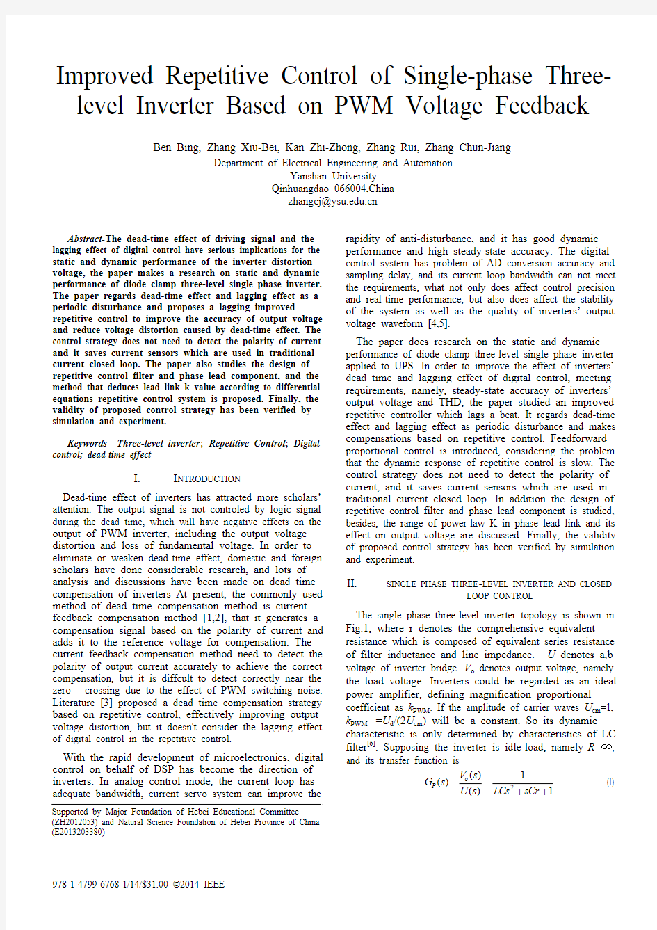
The single phase three-level inverter topology is shown in Fig.1, where r denotes the comprehensive equivalent resistance which is composed of equivalent series resistance of filter inductance and line impedance. U denotes a,b voltage of inverter bridge. V o denotes output voltage, namely the load voltage. Inverters could be regarded as an ideal power amplifier, defining magnification proportional coefficient as k PWM. If the amplitude of carrier waves U cm=1, k PWM=U d/(2U cm) will be a constant. So its dynamic characteristic is only determined by characteristics of LC filter[6]. Supposing the inverter is idle-load, namely R=∞, and its transfer function is
2
()1
()
()1
o
P
V s
G s
U s LCs sCr
==
++
(1)
Supported by Major Foundation of Hebei Educational Committee (ZH2012053) and Natural Science Foundation of Hebei Province of China (E2013203380)
Control block diagram of the inverter is shown in Fig.2.
Where G F1 and G F2 denote feedback coefficient, and G F3(s)
denotes a first-order inertial filtering component implemented by circuit. Considering the dead-time effect of
inverters’ driving signal and switch conduction voltage drop,
PWM pulse of the bridge arm output has loss of voltage, ΔU is regarded as a nonlinear function of output current of the bridge arm i L and dead time T d , namely (,)L d U f i T Δ=, ΔU regarded as disturbance of U
.
Fig. 1 Schematic diagram of single-phase diode-clamped three-level
inverter
U
Fig. 2 Block Diagram of system closed- loops
III. I MPROVED REPETITIVE CONTROL
A. Influence of dead-time effect on output voltage
To avoid the inverter bridge arm "pass-through" phenomenon, setting the dead time, makes two switching devices working in the complementary work state have the simultaneous turn-off time ideally. Simulation is used to study dead time impact on a single-phase three-level inverter, as shown in TABLE I. In TABLE I, U RMS indicates the RMS of inverter output voltage, and lag one beat (50μs ) indicates the time delay caused by signal sampling and calculation process of digital control. With the dead time increasing, the difference of output voltage RMS between idle-load and full-load is bigger, and total harmonic distortion (THD) is larger, so the dead-time effect can make the output characteristics of inverter worse.
Can be seen from TABLE I, when the dead time is set to 2μs , the difference of inverter output RMS between idle-load and full-load is 13V, which does not satisfy the requirements of output voltage regulation accuracy ±2%. In domestic and foreign literature, repetitive control method is used to eliminate the dead-time effect and the influence of the inverter output voltage cuased by rectifier load and other periodic disturbance [7,8], but its dynamic
performance is poorer, so this paper uses the parallel control strategy of repetitive controller and proportional controller, as shown in Fig.3. TABLE I DEAD BAND TIME EFFECT ON INVERTER OUTPUT VOLTAGE
Lag 1 beat
(50μs) Dead zone /0μs Dead zone /2μs Dead zone /4μs
URMS (V) THD (%) URMS (V) THD(%) URMS (V) THD (%)
Idle-load 220.6 0.63 220.6 1.57 220.2 2.17 Full-load 213.9 0.57 207.6 1.06 202.2 2.20
The proportional controller is used to improve the
dynamic performance. Although the resulting voltage error e (z ) error is larger when load mutation error, but the repetitive control lags for a power frequency cycle for disturbance response time. Anti transient disturbance of inverter system is mainly produced by proportional controller, and the teady-state accuracy of inverter voltage is improved by repetitive controller, and the THD of output voltage is reduced, the quality of waveform is optimized.
Fig. 3 Parallel of the proportion and repetitive controller
B. Improved repetitive control and design
According to Fig.3, the transfer function of conventional repetitive controller is
()()
()1()N N
u z z C z e z F z z ?=? (2) The repetitive controller in Fig.3 is not considered the influence of lag one beat caused by digital control delay. If taking the calculation delay time into consideration as one sampling period, which equivalents to join lagging link -1z into the closed loop, and eventually the control block diagram of improved repetitive controller is shown in Fig.4, in which the repeat factor is (1)()N F z z ?
+.
Fig.4 proposed advanced 1 step repetitive and proportional control
From Fig.4, the transfer function of improved repetitive controller is
+11
()()0.8()()1()10.95N N k
N N u z z C z z z S z e z F z z z ?????==??()
(3) where, 0.8r k =, (
)0.95F z =.
In order to make the repetitive control system has better stability and smaller steady-state error, need to design compensator C (z ). From the view point of amplitude phase frequency characteristics, compensator is designed to make C (z )G p (z ) in low and middle frequency band with zero gain zero phase shift and in high frequency band with rapid attenuation characteristics [11,12].
This paper takes the amplitude and phase compensation method respectively, the compensator is designed in two parts: firstly design the filter S (z ) to realize low frequency zero gain and high frequency attenuation characteristics, should have good filtering effect , the gain in low and middle frequency band has little change, attenuation ratio in high-frequency is 40dB/dec; gain in intermediate-frequency is not changeable, attenuation in high-frequency is 40dB/dec; secondly design the lead link z k to realize C (z )G p (z ) zero phase shift characteristics. 1) The design of filter S(z)
The parameters of the inverter filter are given as follows: L =1.2mH, C =15μF, 0.3r =Ω. The sampling period is chosen as T s =50μs according to the inverter switching frequency. From (1), the Z transform transfer function G P (z ) of LC filter can be obtained as (5), where ω0 is the natural resonant frequency.
12
212()P b z b G z
z a
z a +=?+ (4)
where, 0
1
2
ωξ=
=01202212cos(),sin()
1()
()
2s
T
s s e T T b b a a ξωωωαβωγωξω
αβγωξω
ααγβω
αβα?=====?+=+?=?=
The series S (z ) of comb filter S x (z ) and second-order low
pass filter S 1(z ) is a doped to achieve not only eliminate the
resonant peak of LC filter amplitude frequency characteristic, but also make sure the filter zero gain characteristic in the low frequency, in which S x (z ) has a very
strong attenuation effect on a particular frequency and has
zero phase shift characteristics. The Z transform transfer
function of the comb filter choosen is shown as (5).
4
2)(m m x z z z S ?++=
(5) where, m is a positive integer. Then the m value is determined according to the amplitude frequency
characteristic of S x (z ) shown as follows
21()(1cos())42
s
s
s
jT m jT m jT x s e e S e T m ωωω
ω??++==+ (6) When 0/()s m T πω=, then ()0x S z =, it can choose m=8 according to the specific value of 0s T ω given above, The
angular frequency of the first trough points in the amplitude frequency characteristic of S x (z ) is the resonant angular frequency of LC filter. It can eliminate resonance peak of the inverter filter completely in theory, however in fact, the filter inductance value of inverter may varies with output current, the filtering effect of comb filter will reduce.
Design the second-order low pass filter S 1(z ) and it’s parameters. Make the damping ratio ξ=1, choose the natural frequency which is same to the LC filter resonance angle frequency ω0. The Z transform transfer function is shown as follows
000003
4
1234
3040234()1(1)(1)2s s s s
s
T s T T s T T b z b S z z a z a b e T b e e T a e a e ωωωωωωω?????+=?+=?+=++?=?= (7)
Compare the bode of filter S (z ) and S 1(z ) in Fig.5 we can see that the filter S (z ) can eliminate the resonance peak of LC filter and has little attenuation effect on signals in low and middle frequency band.
M a g n i t u d e (d B )
P h
a s e (d e g
)
Fig.5 Bode of filter S(z) and S1(z)
Introduce the gain kr in order to control the output
strength of the compensator C (z ), the final transfer function of compensator can be written as
88342
34()()
24k r k
r C z k z S z b z b z z k z z a z a ?=+++=?+ (8) where z k is the phase lead link, it not only compensate the phase lag caused by the filter S (z ), but also the phase lag caused by the filter G P (z ). In some literature the value of k is choosed generally according to the Bode diagram [11,12],
the method that deduces lead link k value according to
differential equations repetitive control system is proposed. 2) Design of lead link z k After substituting (8) into (2), the transfer function between the compensator output ()u z and the error ()e z in traditional repetitive control is shown as follows
-1-234-1-234()()
()1()0.824
10.951N N
N k m m N u z z C z e z F z z b z b z z z z z z a z a z ?????=
?+++=
?++ (9)
In (9), choose kr=0.8, F (z )=0.95. When realize repetitive
controller, need reserve computer storage space for storage the error e calculated each sampling and the compensator output u . The lowest order absolute value of z, which is in the molecular and denominator polynomial of (9) , plus 1 equals to the number of storage unit which is set by saving error e and the value of the compensator output u, namely the maximum value of 3N +or m+2-k+1N +. Select the k value to ensure the lowest order of z in (10) numerator polynomial should meet -(2)-(2)k N m N ++≤+, then
k m ≤.
Select k =7,6 respectively, achieve the traditional repetitive controller according to (9), the experimental waveforms of inverter output voltage are shown in Fig.6. It can be seen that the voltage waveform is not ideal and the
zero-crossing distortion is serious.
Only reduce the k value for improving the effect of the inverter output waveform is not obvious.
u (10V /
d i
v
)
(a) k=7
(b) k=6
Fig. 6 Output voltage waveform in conventional repetitive control
Select k=7,6 respectively, achieve the improved repetitive controller according to (3), the experimental waveforms of
inverter output voltage are shown in Fig.7, compared with
Fig.6, the voltage waveform is improved significantly.
(a) k=7
(b) k=6
Fig. 7 Output voltage waveform in the proposed repetitive control
It shows that the design of the repetitive control compensator is reasonable, stability is good, the improved repetitive control can improve the dead time effect, it also shows that the validity of the method calculating the maximum value of phase lead compensation k.
IV.
S IMULATION AND E XPERIMENT A NALYSIS
According to the above parameters of the controller and LC filter, it verifies the theory from four aspects, in which all the dead time is 2μs .
1) Rejection disturbance of DC Bus voltage fluctuation The simulation result about the DC Bus voltage varied from 760V to 850V is shown in TABLE Ⅱ. In TABLE Ⅱ IM is the abbreviations of improved repetitive .IR mains the largest difference of inverter output voltage RMS is 6.7V under the proportional control; and the largest RMS output voltage difference is 2.5V under the improved repetitive Control. It shows that the rejection disturbance of DC Bus voltage fluctuation ability of improved repetitive Control is better than that of the proportional control.
TABLE Ⅱ
C OMPARISON OF REJECTION DISTURBANCE OF DC BUS FLUCTUATION AND
LOAD CHANGE Effective
value (V) Load Controller
DC Bus voltage 760(V) 800(V) 850(V) Output voltage 0
Proportional 218.6 221.7 225.3 Proportional+IR 221.4 222.5 223.8 Output voltage
3kw
Proportional 209.2 212.1 215.5 Proportional+IR 216.5 217.6 219
2) Rejection disturbance of load change
When the DC Bus voltage is 800V and the load changed from 0 to 3kw, the difference of inverter output voltage RMS is 9.6V under the proportional control; and the RMS output voltage difference is 4.9V under the improved repetitive control. It shows that rejection disturbance of load change ability of improved repetitive control is better than that of the proportional control. The improved repetitive control under dual voltage closed-loop compensates the influence caused by dead time, and reduces the loss of output voltage amplitude. 3) Dynamic Performance
At t =0.305s, add 3kw resistive load suddenly, and at t =0.505s, reduce 3kw resistive load suddenly, the waveform
of output voltage is shown in Fig.8. It can see that the system recover time decreased and did not have overshoot phenomenon when the load changed suddenly, and the system have a better stablity, it shows that the proposed control of improved repetitive control under dual voltage
closed-loop has a better dynamic performance and stablity.
s
/t V
/
u
Fig. 8 Steady state and transient response of output voltage in the proposed
control method
4) Output voltage THD
Fig.9 and TABLE Ⅲ shows the idle-load and 3kw load experiment results under the two different control methods: proportional control and improved proportional repetitive control paralleled.
TABLE Ⅲ
OUTPUT VOLTAGE THD IN TWO DIFFERENT METHODS
Controller Output voltage(V) THD under 3kw
Load(%)
Proportional 212.1 1.6 Proportional+IR 217.6
1.4
u
(
10
0V /d i
v )
i (18A /d i v
)
(a) Dual voltage feedback proportion control method
u
(
1
V
/d i v )
i
(18A /d i v )
(b) Proposed proportion and repetitive control method Fig. 9 steady state voltage and current waveform with 3kw load
From Fig.9 it can see that although the output voltage and current are in phase under the two different control methods, but TABLE Ⅲ shows that the output voltage THD of improved repetitive control is smaller than that of proportional control, it illustrates that the improved repetitive control decreased the influence caused by dead time.
V.
C ONCLUSION
Considered that time delay effect caused by digital control, the improved repetitive control is propsed to compensate the influence of dead time effect, the paralleled control method of proportional control and improved repetitive control can make up for the inadequacy repetitive control dynamic response slow, and the output voltage quality of the system has obvious improvement, for the THD=1.4%. Besides, the output voltage loss reduced obviously and increased the voltage regulation accuracy under the idle-load and load . The proposed proportional repetitive control does not need detect the polarity of the current, and it saves current sensors which are used in traditional current closed loop, it can achieve faster dynamic performance and higher steady accuracy.
References
[1] Xie meng, Cai Kun, Sheng Xiaosong, et al, “Output Control and
Parallel Operation Control of 400Hz Single-phase Voltage-source Inverter,” Proceeding of the CSEE, vol.26, pp.78-81, 2006.
[2] Xiong Jian, Zhou Liang, Zhang Kaiet al, “A High Percision Multi-loop Control Strategy for Single-phase PWM Inverter,” Transactions of China Electrotechnical Society, vol.21, pp. 79-83, 2006.
[3] Peng Li, Zhang Kai, Kang Yong, et al, “Performance Analysis and
Improvement of Digital Controlled PWM Inverter,”Proceeding of the CSEE, vol.26, pp.65-70, 2006.
[4] Liu Jian, Yin Xianggen, Zhang Zhe, et al, “Study of SPWM Digital
Technologies for High-voltage High-power Three-level NPC Inverter,” Proceeding of the CSEE, vol.28, pp. 35-40, 2008.
[5] Huang Lipei, Liu Yadong, “Research on Digital Control for UPS
Inverter,” Power Electronics, vol.6, pp.7-8, 2008.
[6] Mao Huifeng, Cheng Zenglu, Yang Xu, et al, “Digital Control
Technology for High-pecision and Wide-band Inverter,” Power Electronics, vol.45, pp.75-77, 2011.
[7] Doh Tae-Yong, Ryoo Jung Rae, “Add-on type repetitive controller
design for the feedback control system satisfying the robust performance condition,” Proceedings of 2009 7th Asian Control Conference, pp.1582-1587, 2009.
[8] Xiong Jian, Shi Pengfei, Zhang Kai, et al, “Voltage Differential
Feedback Control Plus Repetitive Control for PWM Inverters,” Advanced Technology of Electrical Engineering and Energy, vol.21, pp.1-4, 2002.
[9] Duan Shanxu, Sun Zhaohui, Zhang Kai, et al, “A Compensation
Strategy for Dead-Time Effect of SPWM Inverters Based on Repetitive Control[J].Transactions of China Electrotechnical Society, vol.19, pp. 52-57, 2004.
[10] Thomas J Manayathara, Tsu-Chin Tsao, Joseph Bentsman, Douglas
Ross, “Rejection of Unknown Periodic Load Disturbances in Continuous Steel Casting Process Using Learning Repetitive Control Approach,” IEEE Transactions on Control Systems Technology, vol.4, pp.259-265, 1996.
[11] Liao Hui, Qiu Shuisheng, Tu Yongjun, et al, “Repetitive Plus PD
Combined Control for Output Voltage of Single-Phase UPS,” Electric Machines & Control Application, vol.36, pp.18-22, 2009.
Gnoatto Claudio Lucas, Scarmin Alcir, Carati Emerson Giovani, “Repetitive Control Techniques Applied to Uninterruptible Power Supplies,” 2010 9th IEEE/IAS International Conference on Industry Applications, 2010.
相关文档
- CP控制计划controlplan培训内容ppt
- 控制计划control plan标准格式及注解
- Quality Control Plan(质量控制计划)
- 很好的--Quality_Control_Plan(质量控制计划)(1)
- 质量控制计划ControlPlan培训教材
- Control Plan 控制计划
- 04_Pre-launch control plan(试生产控制计划)
- ControlPlan控制计划样本
- 控制计划controlplan共20页文档
- 质量控制计划control plan
- Control_Plan控制计划表格
- control plan (控制计划)
- Control_Plan控制计划
- control plan控制计划模板
- CP控制计划(control plan培训内容)
- 控制计划范例Control plan
- Control Plan控制计划
- 控制计划Control_Plan经典讲解
- 控制计划Control_Plan经典讲解
- CONTROL PLAN 过程控制计划