CY7C1061BV33-10ZC中文资料
16-Mbit (1M x 16) Static RAM
CY7C1061BV33
Features
?High speed —t AA = 10 ns ?Low active power —990 mW (max.)
?Operating voltages of 3.3 ± 0.3V ?2.0V data retention
?Automatic power-down when deselected ?TTL-compatible inputs and outputs
?Available in Pb-free and non Pb-free 54-pin TSOP II package
Functional Description
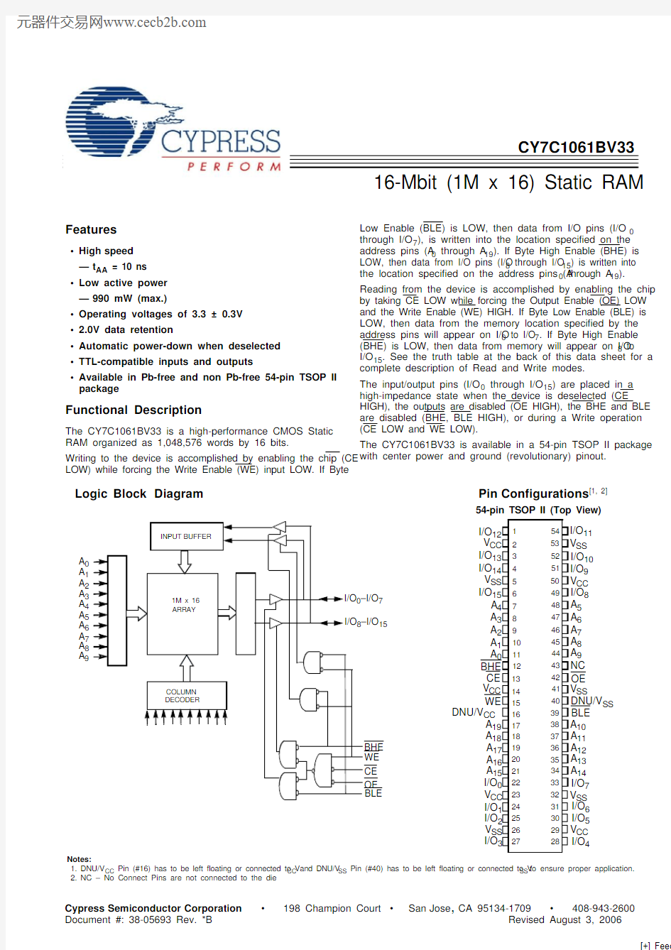
The CY7C1061BV33 is a high-performance CMOS Static RAM organized as 1,048,576 words by 16 bits.
Writing to the device is accomplished by enabling the chip (CE
LOW) while forcing the Write Enable (WE) input LOW. If Byte
Low Enable (BLE) is LOW, then data from I/O pins (I/O 0through I/O 7), is written into the location specified on the address pins (A 0 through A 19). If Byte High Enable (BHE) is LOW, then data from I/O pins (I/O 8 through I/O 15) is written into the location specified on the address pins (A 0 through A 19).Reading from the device is accomplished by enabling the chip by taking CE LOW while forcing the Output Enable (OE) LOW and the Write Enable (WE) HIGH. If Byte Low Enable (BLE) is LOW, then data from the memory location specified by the address pins will appear on I/O 0 to I/O 7. If Byte High Enable (BHE) is LOW, then data from memory will appear on I/O 8 to I/O 15. See the truth table at the back of this data sheet for a complete description of Read and Write modes.
The input/output pins (I/O 0 through I/O 15) are placed in a high-impedance state when the device is deselected (CE HIGH), the outputs are disabled (OE HIGH), the BHE and BLE are disabled (BHE, BLE HIGH), or during a Write operation (CE LOW and WE LOW).
The CY7C1061BV33 is available in a 54-pin TSOP II package with center power and ground (revolutionary) pinout.
Logic Block Diagram 1516A 1A 2A 3A 4A 5A 6A 7A 8COLUMN DECODER
R O W D E C O D E R
S E N S E A M P S
INPUT BUFFER
1M x 16ARRAY
A 0A 12A 14A 13A A A 17A 18A 10A 11I/O 0–I/O 7OE I/O 8–I/O 15
CE WE BLE
BHE A 9
A 19
WE
12345678910111431323635343337403938121341434216152930A 5A 6A 7A 8A 0A 1OE V SS A 17I/O 15A 2CE I/O 2I/O 0I/O 1BHE A 3A 418172019I/O 3
27
28
252622212324I/O 6I/O 4
I/O 5I/O 7A 16A 15BLE V CC I/O 14I/O 13I/O 12I/O 10I/O 9I/O 8A 14A 13A 12A 11A 9A 104446454750494851535254V SS V CC A 19A 18V CC V CC V SS V SS
NC V CC I/O 11V SS DNU/V CC
DNU/V SS 54-pin TSOP II (Top View)
Notes:
1.DNU/V CC Pin (#16) has to be left floating or connected to V CC and DNU/V SS Pin (#40) has to be left floating or connected to V SS to ensure proper application.
2.NC – No Connect Pins are not connected to the die
Pin Configurations [1, 2]
CY7C1061BV33
Maximum Ratings
(Above which the useful life may be impaired. For user guide-lines, not tested.)
Storage Temperature .................................–65°C to +150°C Ambient Temperature with
Power Applied.............................................–55°C to +125°C Supply Voltage on V CC to Relative GND[3]–0.5V to +4.6VDC Voltage Applied to Outputs
in High-Z State[3]....................................–0.5V to V CC + 0.5V DC Input Voltage[3]................................–0.5V to V CC + 0.5V Current into Outputs (LOW).........................................20 mA
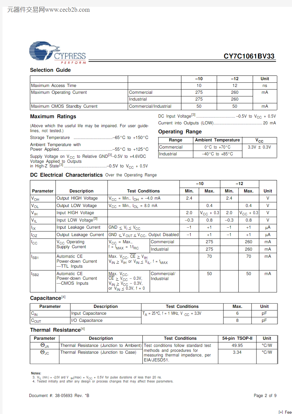
Selection Guide
–10–12Unit Maximum Access Time1012ns Maximum Operating Current Commercial275260mA
Industrial275260
Maximum CMOS Standby Current Commercial/Industrial5050mA
Operating Range
Range Ambient Temperature V CC
Commercial0°C to +70°C 3.3V ± 0.3V
Industrial–40°C to +85°C
DC Electrical Characteristics Over the Operating Range
Parameter Description Test Conditions
–10–12
Unit Min.Max.Min.Max.
V OH Output HIGH Voltage V CC = Min., I OH = –4.0 mA 2.4 2.4V V OL Output LOW Voltage V CC = Min., I OL = 8.0 mA0.40.4V V IH Input HIGH Voltage 2.0V CC + 0.3 2.0V CC + 0.3V V IL Input LOW Voltage[3]–0.30.8–0.30.8V I IX Input Leakage Current GND < V I < V CC–1+1–1+1μA I OZ Output Leakage Current GND < V OUT < V CC, Output Disabled–1+1–1+1μA
I CC V CC Operating
Supply Current V CC = Max.,
f = f MAX = 1/t RC
Commercial275260mA
Industrial275260mA
I SB1Automatic CE
Power-down Current
—TTL Inputs Max. V CC, CE > V IH
V IN > V IH or V IN < V IL, f = f MAX
7070mA
I SB2Automatic CE
Power-down Current
—CMOS Inputs Max. V CC,
CE > V CC – 0.3V,
V IN > V CC – 0.3V,
or V IN < 0.3V, f = 0
Commercial/
Industrial
5050mA
Capacitance[4]
Parameter Description Test Conditions Max.Unit C IN Input Capacitance T A = 25°C, f = 1 MHz, V CC = 3.3V6pF C OUT I/O Capacitance8pF
Thermal Resistance[4]
Parameter Description Test Conditions54-pin TSOP-II Unit
ΘJA Thermal Resistance (Junction to Ambient)Test conditions follow standard test
methods and procedures for
measuring thermal impedance, per
EIA/JESD51.49.95°C/W
ΘJC Thermal Resistance (Junction to Case) 3.34°C/W Notes:
3.V IL (min.) = –2.0V and V IH(max) = V CC + 0.5V for pulse durations of less than 20 ns.
4.Tested initially and after any design or process changes that may affect these parameters.
CY7C1061BV33
AC Test Loads and Waveforms [5]
AC Switching Characteristics Over the Operating Range [6]
Parameter Description
–10
–12
Unit
Min.
Max.
Min.
Max.
Read Cycle t power V CC (typical) to the first access [7]11ms t RC Read Cycle Time 10
12
ns t AA Address to Data Valid
10
12
ns t OHA Data Hold from Address Change 3
3
ns t ACE CE LOW to Data Valid 1012ns t DOE OE LOW to Data Valid 5
6
ns t LZOE OE LOW to Low-Z 1
1
ns t HZOE OE HIGH to High-Z [8]5
6
ns t LZCE CE LOW to Low-Z [8]3
3
ns t HZCE CE HIGH to High-Z [8]5
6
ns t PU CE LOW to Power-Up [9]0
ns t PD CE HIGH to Power-Down [9]1012ns t DBE Byte Enable to Data Valid 5
6
ns t LZBE Byte Enable to Low-Z 1
1
ns t HZBE
Byte Disable to High-Z
5
6
ns
Notes:
5.Valid SRAM operation does not occur until the power supplies have reached the minimum operating V DD (3.0V). As soon as 1ms (T power ) after reaching the minimum operating V DD , normal SRAM operation can begin including reduction in V DD to the data retention (V CCDR , 2.0V) voltage.
6.Test conditions assume signal transition time of 3 ns or less, timing reference levels of 1.5V, input pulse levels of 0 to 3.0V, and output loading of the specified I OL /I OH and specified transmission line loads. T est conditions for the Read cycle use output loading shown in part a) of the AC test loads, unless specified otherwise.
7.This part has a voltage regulator which steps down the voltage from 3V to 2V internally. t power time has to be provided initially before a Read/Write operation is started.
8.t HZOE , t HZCE , t HZWE , t HZBE and t LZOE , t LZCE , t \LZWE , t LZBE are specified with a load capacitance of 5 pF as in (b) of AC T est Loads. Transition is measured ±200 mV from steady-state voltage.
9.These parameters are guaranteed by design and are not tested.
10.The internal Write time of the memory is defined by the overlap of CE LOW and WE LOW. Chip enables must be active and WE and byte enables must be LOW to
initiate a Write, and the transition of any of these signals can terminate the Write. The input data set-up and hold timing should be referenced to the leading edge of the signal that terminates the Write.
11.The minimum Write cycle time for Write Cycle No. 3 (WE controlled, OE LOW) is the sum of t HZWE and t SD .
90%10%
3.3V GND 90%10%
ALL INPUT PULSES
3.3V OUTPUT
5 pF*
INCLUDING JIG AND SCOPE
(a)
(b)
R1 317?
R2351?
Rise time > 1V/ns
Fall time: > 1V/ns
(c)
OUTPUT
50?
Z 0= 50?
V TH = 1.5V
30 pF*
* Capacitive Load consists of all com-ponents of the test environment.
CY7C1061BV33
Write Cycle [10, 11]t WC Write Cycle Time 1012ns t SCE CE LOW to Write End 78ns t AW Address Set-up to Write End 77ns t SA Address Set-up to Write Start 00ns t PWE WE Pulse Width 78ns t SD Data Set-up to Write End 5.56ns t HD Data Hold from Write End 00ns t LZWE WE HIGH to Low-Z [8]3
3
ns t HZWE WE LOW to High-Z [8]5
6
ns t BW Byte Enable to End of Write 78ns t HA
Address Hold from Write End
00
ns
AC Switching Characteristics Over the Operating Range [6] (continued)
Parameter Description
–10
–12Unit Min.
Max.
Min.Max.
Data Retention Waveform
3.0V 3.0V t CDR
V DR >2V
DATA RETENTION MODE
t R
CE
V CC Switching Waveforms
Read Cycle No. 1[12, 13]
Notes:
12.Device is continuously selected. OE, CE, BHE and/or BHE = V IL . 13.WE is HIGH for Read cycle.
PREVIOUS DATA VALID
DATA VALID
t RC
t AA
t OHA
ADDRESS
DATA OUT
CY7C1061BV33
Read Cycle No. 2 (OE Controlled)[13, 14]
Write Cycle No. 1 (CE Controlled)[15, 16]
Notes:
14.Address valid prior to or coincident with CE transition LOW.15.Data I/O is high-impedance if OE or BHE and/or BLE = V IH .
16.If CE goes HIGH simultaneously with WE going HIGH, the output remains in a high-impedance state.
Switching Waveforms (continued)
50%
50%
DATA VALID
t RC
t ACE
t DOE t LZOE t LZCE t PU
HIGH IMPEDANCE
t HZOE
t HZBE
t PD
HIGH OE CE
ICC IMPEDANCE
ADDRESS
DATA OUT V CC SUPPLY t DBE t LZBE
t HZCE BHE,BLE
CURRENT
I CC I SB
t HD
t SD
t SCE
t SA t HA
t AW
t PWE
t WC
BW
DATAI/O
ADDRESS
CE
WE
BHE,BLE
t
CY7C1061BV33
Write Cycle No. 2 (BLE or BHE Controlled)
Write Cycle No. 3 (WE Controlled, OE LOW)[15, 16]
Switching Waveforms (continued)
t HD
t SD
t BW
t SA t HA
t AW
t PWE
t WC
t SCE
DATAI/O
ADDRESS
BHE,BLE
WE
CE
t HD
t SD
t SCE
t HA
t AW
t PWE
t WC
t BW
DATA I/O
ADDRESS
CE
WE
BHE,BLE
t SA
t LZWE
t HZWE
CY7C1061BV33 Truth Table
CE OE WE BLE BHE I/O0–I/O7I/O8–I/O15Mode Power
H X X X X High-Z High-Z Power-down Standby (I SB)
L L H L L Data Out Data Out Read All Bits Active (I CC) L L H L H Data Out High-Z Read Lower Bits Only Active (I CC) L L H H L High-Z Data Out Read Upper Bits Only Active (I CC) L X L L L Data In Data In Write All Bits Active (I CC) L X L L H Data In High-Z Write Lower Bits Only Active (I CC) L X L H L High-Z Data In Write Upper Bits Only Active (I CC) L H H X X High-Z High-Z Selected, Outputs Disabled Active (I CC) Ordering Information
Speed
(ns)Ordering Code Package
Name Package Type Operating Range
10CY7C1061BV33-10ZC51-8516054-pin TSOP II Commercial CY7C1061BV33-10ZI Industrial CY7C1061BV33-10ZXC54-pin TSOP II (Pb-free)Commercial CY7C1061BV33-10ZXI Industrial 12CY7C1061BV33-12ZC54-pin TSOP II Commercial CY7C1061BV33-12ZI Industrial CY7C1061BV33-12ZXC54-pin TSOP II (Pb-free)Commercial CY7C1061BV33-12ZXI Industrial
CY7C1061BV33
All products and company names mentioned in this document may be the trademarks of their respective holders.
Package Diagram
51-85160-**
54-pin TSOP II (51-85160)
CY7C1061BV33 Document History Page
Document Title: CY7C1061BV33 16-Mbit (1M x 16) Static RAM
Document Number: 38-05693
REV.ECN NO.Issue Date Orig. of
Change Description of Change
**283950See ECN RKF New data sheet
*A309453See ECN RKF Final data sheet
*B492137See ECN NXR Removed 8 ns speed bin
Changed the description of I IX from Input Load Current to Input Leakage
Current in DC Electrical Characteristics table
Updated the Ordering Information Table