XQ1006-BD-EV1中文资料
Units GHz GHz dBm dBm dBc/Hz dBc/Hz dBc dBc dBc
MHz/Volt
VDC VDC mA
Min.
14.7 1.84---------+1.0
-Typ.--+5.0+2.0-88.0-113.0-35.0-45.0-42.040.0+4.0-110Max.15.71.96---------+6.0130
14.7-15.7 GHz GaAs MMIC Voltage Controlled Oscillator
Features
On-Chip Prescaler
+5.0 dBm Output Power
-35 dBc Harmonic Suppression -88 dBc/Hz @ 100KHz Phase Noise 110mA @ 4.0V Bias Supply
100% On-Wafer, DC and Output Power Testing 100% Visual Inspection to MIL-STD-883Method 2010
General Description
Parameter
Supply Voltage (Vcc1,2,3)Supply Voltage (Vtune)Supply Current (Icc1,2,3)Supply Current (Itune)
Storage Temperature (Tstg)Operating Temperature (Ta)Junction Temperature (Tjn)
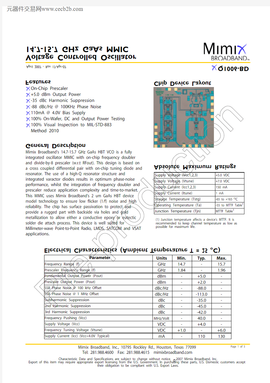
+5.0 VDC +7.0 VDC 150 mA 1 mA -65 to +165 O C -55 to MTTF Table MTTF Table Chip Device Layout
(1) Junction temperature affects a device's MTTF. It is recommended to keep channel temperature as low as possible for maximum life.
1
1Mimix Broadband's 14.7-15.7 GHz GaAs HBT VCO is a fully integrated oscillator MMIC with on-chip frequency doubler and divide-by-8 prescaler (w.r.t RFout). This design is based on a cross coupled differential pair with on-chip tuning diode and resonator. The use of a high-Q resonator structure and integrated varactor diodes results in optimum phase-noise performance, whilst the integration of frequency doubler and prescaler reduce application complexity and time-to-market. This MMIC uses Mimix Broadband's 2 um GaAs HBT device model technology to ensure low flicker (1/f) noise and high reliability. The chip has surface passivation to protect and provide a rugged part with backside via holes and gold metallization to allow either a conductive epoxy or eutectic solder die attach process. This device is well suited for
Millimeter-wave Point-to-Point Radio, LMDS, SATCOM and VSAT applications.
Electrical Characteristics (Ambient T emperature T = 25 o C)
Absolute Maximum Ratings
Frequency Range (f)
Prescaler Frequency Range (f)Fundamental Output Power (Pout)Prescaler Output Power (Pout)SSB Phase Noise @ 100 kHz Offset SSB Phase Noise @ 1 MHz Offset Subharmonic Suppression 2nd Harmonic Suppression 3rd Harmonic Suppression Frequency Pushing (Vcc)Supply Voltage (Vcc)
Frequency Tuning Voltage (Vtune)Supply Current (Icc) (Vcc=4.0V Typical)
April 2007 - Rev 17-Apr-07
X Q 1006-B D
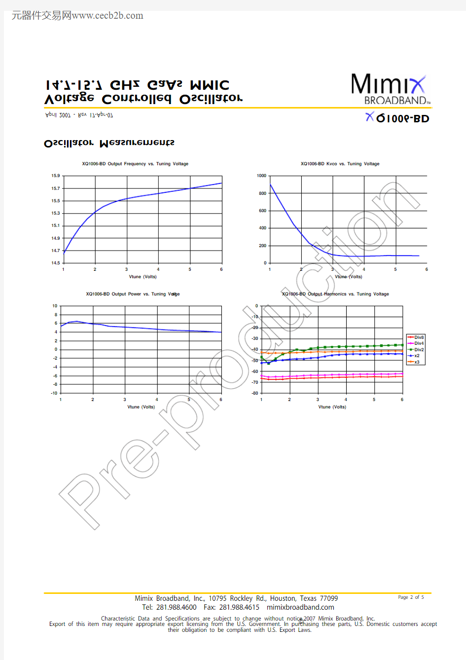
Oscillator Measurements
14.7-15.7 GHz GaAs MMIC Voltage Controlled Oscillator
XQ1006-BD Output Frequency vs. Tuning Voltage
F o u t (
G
H z )
April 2007 - Rev 17-Apr-07
XQ1006-BD Kvco vs. Tuning Voltage
P o u t (d B m )
1
3
2
4
5
6
7
X Q 1006-B D
2.000(0.079)
0.732Mechanical Drawing
14.7-15.7 GHz GaAs MMIC Voltage Controlled Oscillator
April 2007 - Rev 17-Apr-07
App Note [1] Biasing - As shown in the bonding diagram, this device is operated by separately biasing Vcc (1,2,3) and Vtune with Vcc(1,2,3)= +4.0 V and Vtune = +1.0 to +6.0 V, Icc1=30mA, Icc2=10mA, Icc3=70mA.
App Note [2] Bias Arrangement - Each DC pad (Vcc1, 2, 3 and Vtune) needs to have DC bypass capacitance. (~100 - 200 pF, 100pF max on Vtune) as close to the device as possible. Prescaler output (RF Div1, RF Div2) can be used differential or single-end as required.
T
14.7-15.7 GHz GaAs MMIC Voltage Controlled Oscillator
April 2007 - Rev 17-Apr-07
Handling and Assembly Information
CAUTION! - Mimix Broadband MMIC Products contain gallium arsenide (GaAs) which can be hazardous to the human body and the environment. For safety, observe the following procedures:
Do not ingest.
Do not alter the form of this product into a gas, powder, or liquid through burning, crushing, or chemical processing as these by-products are dangerous to the human body if inhaled, ingested, or swallowed.Observe government laws and company regulations when discarding this product. This product must be
discarded in accordance with methods specified by applicable hazardous waste procedures.
14.7-15.7 GHz GaAs MMIC Voltage Controlled Oscillator
Life Support Policy - Mimix Broadband's products are not authorized for use as critical components in life support devices or systems without the express written approval of the President and General Counsel of Mimix
Broadband. As used herein: (1) Life support devices or systems are devices or systems which, (a) are intended for surgical implant into the body, or (b) support or sustain life, and whose failure to perform when properly used in accordance with instructions for use provided in the labeling, can be reasonably expected to result in a
significant injury to the user. (2) A critical component is any component of a life support device or system whose failure to perform can be reasonably expected to cause the failure of the life support device or system, or to affect its safety or effectiveness.
ESD - Gallium Arsenide (GaAs) devices are susceptible to electrostatic and mechanical damage. Die are supplied in antistatic containers, which should be opened in cleanroom conditions at an appropriately grounded anti-static workstation. Devices need careful handling using correctly designed collets, vacuum pickups or, with care,sharp tweezers.
Die Attachment - GaAs Products from Mimix Broadband are 0.100 mm (0.004") thick and have vias through to the backside to enable grounding to the circuit. Microstrip substrates should be brought as close to the die as
possible. The mounting surface should be clean and flat. If using conductive epoxy, recommended epoxies are Tanaka TS3332LD, Die Mat DM6030HK or DM6030HK-Pt cured in a nitrogen atmosphere per manufacturer's cure schedule.Apply epoxy sparingly to avoid getting any on to the top surface of the die. An epoxy fillet should be visible around the total die periphery. For additional information please see the Mimix "Epoxy Specifications for Bare Die" application note.If eutectic mounting is preferred, then a fluxless gold-tin (AuSn) preform, approximately 0.0012 thick, placed between the die and the attachment surface should be used. A die bonder that utilizes a heated collet and provides scrubbing action to ensure total wetting to prevent void formation in a nitrogen atmosphere is recommended. The gold-tin
eutectic (80% Au 20% Sn) has a melting point of approximately 280 oC (Note: Gold Germanium should be avoided). The work station temperature should be 310 oC +/- 10 oC. Exposure to these extreme temperatures should be kept to minimum. The collet should be heated, and the die pre-heated to avoid excessive thermal shock. Avoidance of air bridges and force impact are critical during placement.
Wire Bonding - Windows in the surface passivation above the bond pads are provided to allow wire bonding to the die's gold bond pads. The recommended wire bonding procedure uses 0.076 mm x 0.013 mm (0.003" x
0.0005") 99.99% pure gold ribbon with 0.5-2% elongation to minimize RF port bond inductance. Gold 0.025 mm (0.001") diameter wedge or ball bonds are acceptable for DC Bias connections. Aluminum wire should be
avoided. Thermo-compression bonding is recommended though thermosonic bonding may be used providing the ultrasonic content of the bond is minimized. Bond force, time and ultrasonics are all critical parameters.
Bonds should be made from the bond pads on the die to the package or substrate. All bonds should be as short as possible.
April 2007 - Rev 17-Apr-07
Part Number for Ordering Description
XQ1006-BD-000V Where “V” is RoHS compliant die packed in vacuum release gel paks
XQ1006-BD-EV1
XQ1006 die evaluation module
相关文档
最新文档
- 学校教育环境对学习的影响
- 佳音英语:针对东方的孩子量身定制教材
- 高中语文教学常用网址
- 【2018新浪教育盛典候选机构-万达宝贝王早教】 国剧盛典2018
- “Hereyouare.”用法多新浪教育
- 师德师风心得新浪博客
- 定远县水资源利用和保护探析
- 某化工企业节能减排污染预防与解决环境问题可行性分析
- 双氧水生产工艺及市场分析
- 安徽省环保厅关于对安徽定远盐化工业园等8起环境违法案件实施挂牌督办的通知
- 遍访企业 助力纾困自查报告
- 住房和城乡建设部公告第761号--关于2010年第十六批勘察设计注册工程师初始注册人员名单的公告
- 滁州市承接产业转移示范区建设分报告
- 新型化工产业十四五发展规划
- 快乐的人作文15篇
- 快乐的人作文(通用30篇)
- 一个快乐的人作文
- 最快乐的人作文(精选20篇)
- 一个快乐的人作文14篇
- [作文]一个快乐的人作文15篇