BUZ11中文资料
BUZ11
N -CHANNEL 50V -0.03?-33A TO-220
STripFET ?MOSFET
s TYPICAL R DS(on)=0.03?
s AVALANCHE RUGGED TECHNOLOGY s 100%AVALANCHE TESTED s HIGH CURRENT CAPABILITY
s
175o C OPERATING TEMPERATURE
APPLICATIONS
s HIGH CURRENT,HIGH SPEED SWITCHING s SOLENOID AND RELAY DRIVERS s REGULATORS
s DC-DC &DC-AC CONVERTERS
s MOTOR CONTROL,AUDIO AMPLIFIERS s AUTOMOTIVE ENVIRONMENT (INJECTION,ABS,AIR-BAG,LAMPDRIVERS,Etc.)
?
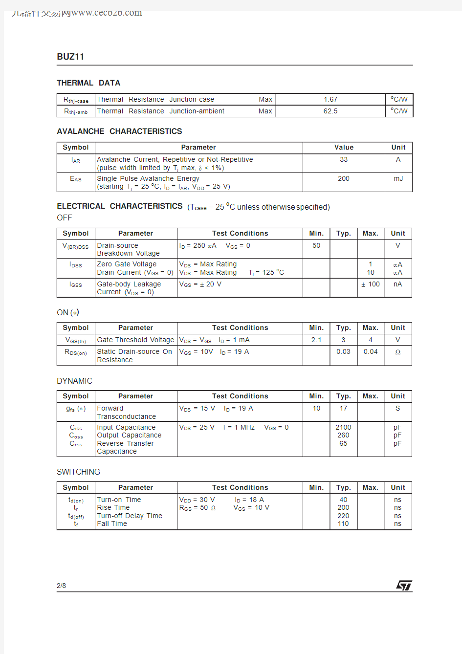
INTERNAL SCHEMATIC DIAGRAM
July 1999123
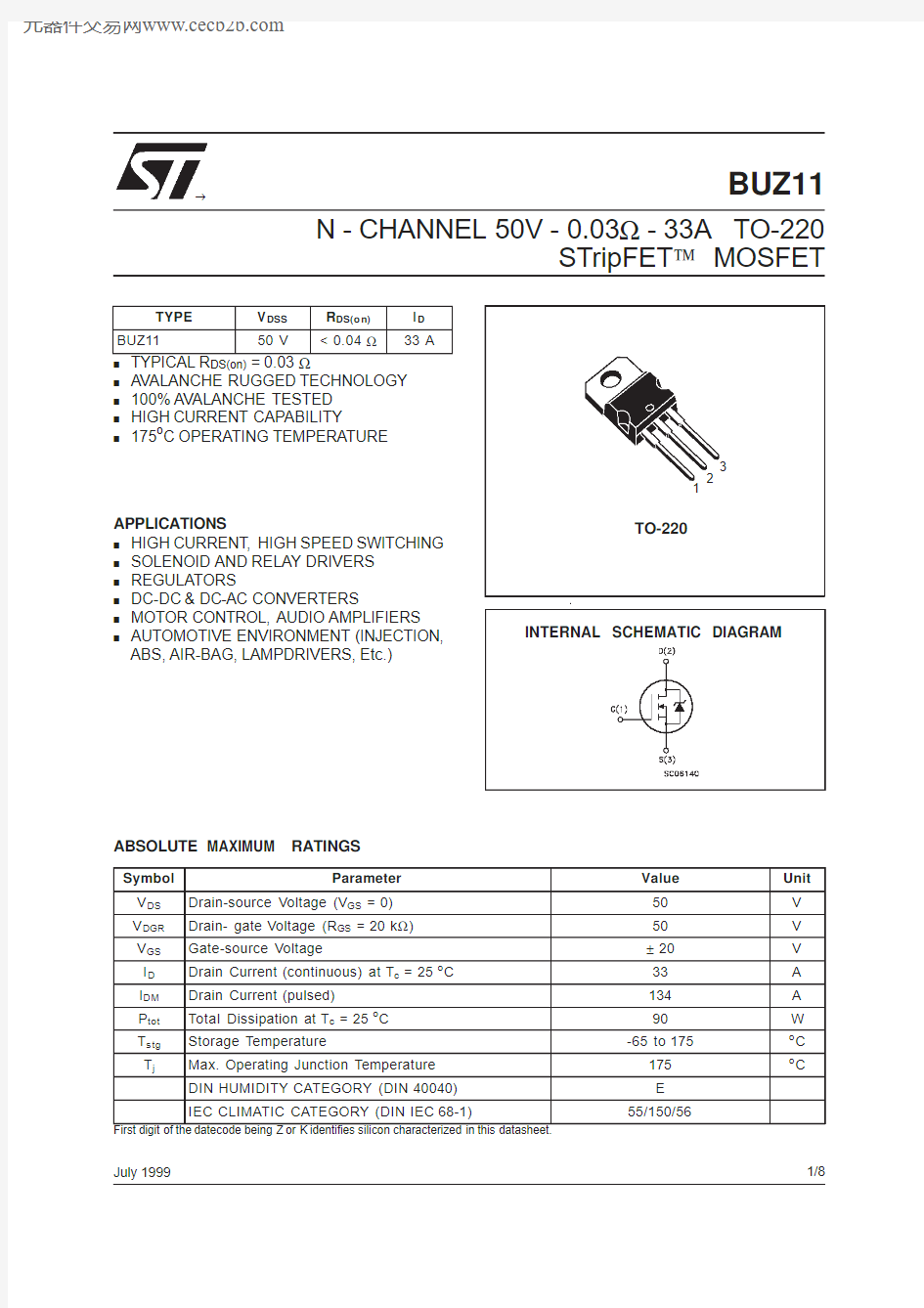
TO-220
ABSOLUTE MAXIMUM RATINGS
Symbol Parameter
Value Unit V DS Drain-source Voltage (V GS =0)50V V DGR Drain-gate Voltage (R GS =20k ?)50V V GS Gate-source Voltage
±20V I D Drain Current (continuous)at T c =25o C 33A I DM Drain Current (pulsed)
134A P tot Total Dissipation at T c =25o C 90W
T s tg Storage Temperature
-65to 175
o C T j
Max.Operating Junction Temperature 175o
C
DIN HUMIDITY CATEGORY (DIN 40040)E IEC CLIMATIC CATEGORY (DIN IEC 68-1)
55/150/56
First digit of the datecode being Z or K identifies silicon characterized in this datasheet.
TYPE V DSS R DS(o n)I D BUZ11
50V
<0.04?
33A
1/8
THERMAL DATA
R thj-case Thermal Resistance Junction-case Max 1.67o C/W R thj-amb Thermal Resistance Junction-ambient Max62.5o C/W
AVALANCHE CHARACTERISTICS
Symbol Parameter Value Unit
I AR Avalanche Current,Repetitive or Not-Repetitive
(pulse width limited by T j max,δ <1%)
33A
E AS Single Pulse Avalanche Energy
(starting T j=25o C,I D=I AR,V DD=25V)
200mJ
ELECTRICAL CHARACTERISTICS(T case=25o C unless otherwise specified)
OFF
Symbol Parameter Test Conditions Min.Typ.Max.Unit V(BR)DSS Drain-source
Breakdown Voltage
I D=250μA V GS=050V
I DSS Zero Gate Voltage
Drain Current(V GS=0)V DS=Max Rating
V DS=Max Rating T j=125o C
1
10
μA
μA
I GSS Gate-body Leakage
Current(V DS=0)
V GS=±20V±100nA ON(?)
Symbol Parameter Test Conditions Min.Typ.Max.Unit V GS(th)Gate Threshold Voltage V DS=V GS I D=1mA 2.134V R DS(on)Static Drain-source On
Resistance
V GS=10V I D=19A0.030.04?DYNAMIC
Symbol Parameter Test Conditions Min.Typ.Max.Unit
g f s(?)Forward
Transconductance
V DS=15V I D=19A1017S
C iss C os s C rss Input Capacitance
Output Capacitance
Reverse Transfer
Capacitance
V DS=25V f=1MHz V GS=02100
260
65
pF
pF
pF
SWITCHING
Symbol Parameter Test Conditions Min.Typ.Max.Unit
t d(on) t r t d(of f) t f Turn-on Time
Rise Time
Turn-off Delay Time
Fall Time
V DD=30V I D=18A
R GS=50 ?V GS=10V
40
200
220
110
ns
ns
ns
ns
BUZ11 2/8
ELECTRICAL CHARACTERISTICS(continued)
SOURCE DRAIN DIODE
Symbol Parameter Test Conditions Min.Typ.Max.Unit
I SD I SDM Source-drain Current
Source-drain Current
(pulsed)
33
134
A
A
V SD(?)Forward On Voltage I SD=60A V GS=0 1.8V
t rr Q rr Reverse Recovery
Time
Reverse Recovery
Charge
I SD=36A di/dt=100A/μs
V DD=30V T j=150o C
75
0.24
ns
μC
(?)Pulsed:Pulse duration=300μs,duty cycle1.5%
Safe Operating Area Thermal Impedance
BUZ11
3/8
Output Characteristics Transconductance
Gate Charge vs Gate-source Voltage Transfer Characteristics
Static Drain-source On Resistance Capacitance Variations
BUZ11 4/8
Normalized Gate Threshold Voltage vs Temperature
Source-drain Diode Forward Characteristics Normalized On Resistance vs Temperature
BUZ11
5/8
Fig.1:Unclamped Inductive Load Test Circuit Fig.3:Switching Times Test Circuits For Resistive Load Fig.2:Unclamped Inductive Waveform Fig.4:Gate Charge test Circuit
Fig.5:Test Circuit For Inductive Load Switching And Diode Recovery Times
BUZ11
6/8
DIM.mm
inch MIN.TYP.
MAX.MIN.TYP.
MAX.A 4.40 4.600.1730.181C 1.23 1.320.0480.051D 2.40
2.72
0.094
0.107
D1 1.27
0.050
E 0.490.700.0190.027
F 0.610.880.0240.034F1 1.14 1.700.0440.067F2 1.14 1.700.0440.067
G 4.95 5.150.1940.203G1 2.4 2.70.0940.106H210.0
10.40
0.393
0.409
L216.4
0.645
L413.014.00.5110.551L5 2.65 2.950.1040.116L615.2515.750.6000.620L7 6.2 6.60.2440.260L9 3.5 3.930.1370.154DIA.
3.75 3.85
0.147
0.151
L6
A
C
D
E
D 1
F
G
L7
L2
Dia.
F 1
L5
L4
H 2
L9
F 2
G 1
TO-220MECHANICAL DATA
P011C
BUZ11
7/8
Information furnished is believed to be accurate and reliable.However,STMicroelect r onics assumes no responsibility for the consequences of use of such information nor for any infringement of patents or other rights of third part i es which may result from its use.No license is granted by implication or otherwise under any patent or patent rights of STMicroelectro nics.Specification mentioned in this publication are subject to change without notice.This publication supersedes and replaces all informat i on previously supplied.STMicroelectronics products are not authorized for use as critical components in life support devices or systems with out express written approval of STMicroelectronics.
The ST logo is a trademark of STMicroelectronics
?1999STMicroelectronics –Printed in Italy –All Rights Reserved
STMicroelectronics GROUP OF COMPANIES
Australia -Brazil -China -Finland -France -Germany -Hong Kong -India -Italy -Japa n -Malaysia -Malta -Morocco -Singapore -Spain -Sweden -Switzerland -United Kingdom -U.S.A.
https://www.sodocs.net/doc/ad717132.html,
.
BUZ11
8/8