MTP3N60中文资料

MTP3N60MTP3N60FI
N -CHANNEL ENHANCEMENT MODE
POWER MOS TRANSISTOR
s TYPICAL R DS(on)=2?
s AVALANCHE RUGGED TECHNOLOGY s 100%AVALANCHE TESTED
s REPETITIVE AVALANCHE DATA AT 100o C s
APPLICATION ORIENTED CHARACTERIZATION
APPLICATIONS s HIGH CURRENT,HIGH SPEED SWITCHING s SWITCH MODE POWER SUPPLIES (SMPS)s CHOPPER REGULATORS,CONVERTERS,MOTOR CONTROL,LIGHTING FOR INDUSTRIAL AND CONSUMER ENVIRONMENT
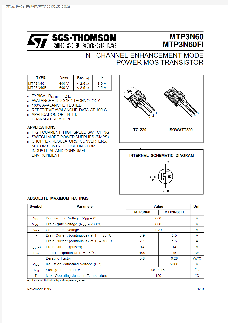
INTERNAL SCHEMATIC DIAGRAM
TYPE V DSS R DS(on)I D MTP3N60MTP3N60FI
600V 600V
<2.5?<2.5?
3.9A 2.5A
1
2
3
TO-220
ISOWATT220
November 1996ABSOLUTE MAXIMUM RATINGS
Symbol Parameter
Value
Unit
MTP3N60
MTP3N60FI
V D S Drain-source Voltage (V GS =0)600V V DG R Drain-gate Voltage (R GS =20k ?)600V V GS Gate-source Voltage
±20
V I D Drain Current (continuous)at T c =25o C 3.9 2.5A I D Drain Current (continuous)at T c =100o C 2.4 1.5A I D M (?)Drain Current (pulsed)
1414A P tot Total Dissipation at T c =25o C 10035W Derating Factor
0.80.28W/o C V ISO Insulation Withstand Voltage (DC)
2000
V
T stg Storage Temperature
-65to 150
o C T j
Max.Operating Junction Temperature
150o
C
(?)Pulse width limited by safe operating area
12
3
1/10
THERMAL DATA
TO-220ISOWATT220
R thj-cas e Thermal Resistance Junction-case Max 1.25 3.57o C/W
R thj-amb R t hc-sin k
T l Thermal Resistance Junction-ambient Max
Thermal Resistance Case-sink Typ
Maximum Lead Temperature For Soldering Purpose
62.5
0.5
300
o C/W
o C/W
o C
AVALANCHE CHARACTERISTICS
Symbol Parameter Max Value Unit
I A R Avalanche Current,Repetitive or Not-Repetitive
(pulse width limited by T j max,δ <1%)
3.9A
E AS Single Pulse Avalanche Energy
(starting T j=25o C,I D=I AR,V D D=25V)
300mJ
E AR Repetitive Avalanche Energy
(pulse width limited by T j max,δ <1%)
7.7mJ
I A R Avalanche Current,Repetitive or Not-Repetitive
(T c=100o C,pulse width limited by T j max,δ <1%)
2.4A
ELECTRICAL CHARACTERISTICS(T case=25o C unless otherwise specified)
OFF
Symbol Parameter Test Conditions Min.Typ.Max.Unit V(BR)DSS Drain-source
Breakdown Voltage
I D=250μA V G S=0600V
I DS S Zero Gate Voltage
Drain Current(V GS=0)V DS=Max Rating
V DS=Max Rating x0.8T c=125o C
25
250
μA
μA
I G SS Gate-body Leakage
Current(V D S=0)
V GS=±20V±100nA ON(?)
Symbol Parameter Test Conditions Min.Typ.Max.Unit V G S(th)Gate Threshold Voltage V DS=V GS I D=1mA23 4.5V R DS(on)Static Drain-source On
Resistance
V GS=10V I D=1.5A2 2.5?
I D(on)On State Drain Current V DS>I D(on)x R D S(on)max
V GS=10V
3.9A DYNAMIC
Symbol Parameter Test Conditions Min.Typ.Max.Unit
g fs(?)Forward
Transconductance
V DS>I D(on)x R D S(on)max I D=1.5A 1.5 2.6S
C iss C oss C rss Input Capacitance
Output Capacitance
Reverse Transfer
Capacitance
V DS=25V f=1MHz V G S=0560
90
40
800
130
55
pF
pF
pF
MTP3N60/FI 2/10
ELECTRICAL CHARACTERISTICS(continued)
SWITCHING ON
Symbol Parameter Test Conditions Min.Typ.Max.Unit
t d(on) t r Turn-on Time
Rise Time
V DD=225V I D=2.5A
R G=15?V GS=10V
(see test circuit,figure3)
45
33
60
42
ns
ns
(di/dt)on Turn-on Current Slope V DD=480V I D=4A
R G=15?V GS=10V
(see test circuit,figure5)
200A/μs
Q g Q gs Q gd Total Gate Charge
Gate-Source Charge
Gate-Drain Charge
V DD=480V I D=4A V GS=10V43
6
21
55nC
nC
nC
SWITCHING OFF
Symbol Parameter Test Conditions Min.Typ.Max.Unit
t r(Vof f) t f
t c Off-voltage Rise Time
Fall Time
Cross-over Time
V DD=480V I D=4A
R G=15?V GS=10V
(see test circuit,figure5)
35
40
60
45
55
75
ns
ns
ns
SOURCE DRAIN DIODE
Symbol Parameter Test Conditions Min.Typ.Max.Unit
I S D I SDM(?)Source-drain Current
Source-drain Current
(pulsed)
3.9
14
A
A
V S D(?)Forward On Voltage I SD=3.9A V GS=02V
t rr Q rr I RRM Reverse Recovery
Time
Reverse Recovery
Charge
Reverse Recovery
Current
I SD=4A di/dt=100A/μs
V DD=100V T j=150o C
(see test circuit,figure5)
420
3.7
18
ns
μC
A
(?)Pulsed:Pulse duration=300μs,duty cycle1.5%
(?)Pulse width limited by safe operating area
Safe Operating Areas For TO-220Safe Operating Areas For ISOWATT220
MTP3N60/FI
3/10
Thermal Impedeance For TO-220 Derating Curve For TO-220 Output Characteristics Thermal Impedance For ISOWATT220 Derating Curve For ISOWATT220 Transfer Characteristics
MTP3N60/FI 4/10
MTP3N60/FI Transconductance Static Drain-source On Resistance
Gate Charge vs Gate-source Voltage Capacitance Variations
Normalized Gate Threshold Voltage vs
Normalized On Resistance vs Temperature Temperature
5/10
MTP3N60/FI
Turn-on Current Slope Turn-off Drain-source Voltage Slope
Cross-over Time Switching Safe Operating Area
Accidental Overload Area Source-drain Diode Forward Characteristics 6/10
Fig.2:Unclamped Inductive Waveforms
Fig.3:Switching Times Test Circuits For Resistive Load
Fig.4:Gate Charge Test Circuit
Fig.5:Test Circuit For Inductive Load Switching And Diode Reverse Recovery Time
Fig.1:Unclamped Inductive Load Test Circuits
MTP3N60/FI
7/10
DIM.mm
inch MIN.TYP.
MAX.MIN.TYP.
MAX.A 4.40 4.600.1730.181C 1.23 1.320.0480.051D 2.40
2.72
0.094
0.107
D1 1.27
0.050
E 0.490.700.0190.027
F 0.610.880.0240.034F1 1.14 1.700.0440.067F2 1.14 1.700.0440.067
G 4.95 5.150.1940.203G1 2.4 2.70.0940.106H210.0
10.40
0.393
0.409
L216.4
0.645
L413.014.00.5110.551L5 2.65 2.950.1040.116L615.2515.750.6000.620L7 6.2 6.60.2440.260L9 3.5 3.930.1370.154DIA.
3.75 3.85
0.147
0.151
L6
A
C
D
E
D 1
F
G
L7
L2
Dia.
F 1
L5
L4
H 2
L9
F 2
G 1
TO-220MECHANICAL DATA
P011C
MTP3N60/FI
8/10
DIM.
mm inch MIN.
TYP.
MAX.MIN.TYP.
MAX.A 4.4 4.60.1730.181B 2.5 2.70.0980.106D 2.5 2.750.0980.108E 0.40.70.0150.027F 0.7510.0300.039F1 1.15 1.70.0450.067F2 1.15 1.70.0450.067G 4.95 5.20.1950.204G1 2.4 2.70.0940.106H 10
10.4
0.393
0.409
L216
0.630
L328.630.6 1.126 1.204L49.810.60.3850.417L615.916.40.6260.645L799.30.3540.366?
3 3.2
0.118
0.126
L2
A
B
D
E
H
G
L6
?
F
L3
G 1
123
F 2
F 1
L7
L4
ISOWATT220MECHANICAL DATA
P011G
MTP3N60/FI
9/10
MTP3N60/FI
Information furnished is believed to be accur ate and reliable.Howev er,SGS-THOMSON Microelectronics assumes no respon sability for the consequ enc es of use of such information nor for any infringem ent of paten ts or other rights of third parties which may results from its use.No license is grante d by implication or otherwise under any patent or patent rights of SGS-THOMSON Microelec tronics.Specifications mentioned in this publication are subject to chan ge without notice.This publicat ion superse des and replaces all information previou sly supplie d.
SGS-THOMSON Microelec tronics produ cts are not autho rized for use as critical compone nts in lifesupport devic es or system s without expres s written app roval of SGS-THOMSON Microelectonics.
?1996SGS-THOMSON Microele ctronics-Printed in Italy-All Rights Reserve d
SGS-THOMSON Microelectronics GROUP OF COMPANIES
Australia-Brazil-Canada-China-France-Germany-Hong Kong-Italy-Japan-Korea-Malays ia-Malta-Morocco-The Netherlands-Singap ore-Spain-Sweden-Switzerland-Taiwan-Thailand-United Kingdo m-U.S.A
.
10/10